


Mastering PCB Reverse Engineering: A Step-by-Step Guide

Reverse engineering plays a role in many industries and is especially popular for those who utilize printed circuit boards (PCBs) in their work. When using PCB reverse engineering, you can gain crucial information about their function and design, helping you make repairs, upgrade older circuit boards or produce a less-costly alternative to a competitor. By knowing how to reverse engineer PCBs, you can gain a complete understanding of how your PCBs work and reap the many benefits of this process.
Find out more about what reverse engineering means and what the benefits of doing so for your PCBs are by exploring the information below. You’ll also learn about how you can reverse engineer a PCB.
What Does It Mean to Reverse Engineer a PCB?
PCB reverse engineering is a multilayered process that includes targeted PCB research, reverse analysis and PCB design technology reproduction. The process is also used to identify and obtain the design of a product’s functional and structural characteristics, as well as the processing flow. With this information, a company can produce products with similar functions and abilities — though businesses will make sure they’re not reproducing an exact replica of a reverse-engineered PCB.
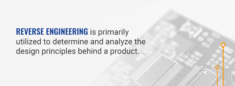
Reverse engineering is primarily utilized to determine and analyze the design principles behind a product. It’s especially useful when a company can’t easily find design information on a specific product.
The most common method of reverse engineering a PCB involves disassembling a sample PCB and then analyzing it. From this analysis, a company will create documentation about the sample PCB, which various team members can review. This documentation will often include information about how the product is designed and how it operates.
A company can then use the information they gather from a sample PCB to manufacture similar PCBs that may function better than their competitors’ offerings. Alongside reverse engineering’s ability to help companies analyze and outdo competitors’ products, it can also help businesses improve their own PCB offerings. For example, reverse engineering can help them enhance their boards’ functionality by spotting obsolete parts, security issues or poor designs.
What Are the Benefits to Reverse Engineering a PCB?
There are several advantages of reverse engineering PCBs — many companies use these devices for various purposes. For example, you may want to reverse engineer a PCB that doesn’t have any documentation or one that’s outdated but still crucial to your processes. Reverse engineering can also help you produce more effective or less costly versions of a competitor’s PCBs.
Learn more about the advantages of reverse engineering PCBs below:
- Maintain crucial PCBs: At times, you may have an outdated PCB that performs a necessary function, such as powering a piece of machinery or an electronic component. If the PCB fails or needs to be replaced, you may not be able to find a replacement or know how to repair it. Reverse engineering the outdated PCB can help you in both these situations, allowing you to maintain crucial PCBs for a long time and potentially clone them to serve as replacements when repairs aren’t possible.
- Get information on PCBs without documentation: Most contemporary PCBs come with documentation or computer-aided design (CAD) data for people to review. Sometimes, PCBs don’t have any information available for them. In this case, reverse engineering is crucial to gather the necessary schematic and design information on the PCB. Reverse engineering allows you to create your own documentation on the product, helping you understand how to repair or reproduce it.
- Reduce your reliance on experts: One of the first steps you’ll probably take when your PCB is having an issue is to contact an expert for help with troubleshooting and repairs. Sometimes, there aren’t any professionals who have the expertise to handle your PCB. This lack of knowledge about the PCB can put you in a bind. Reverse engineering allows you to receive crucial information about your PCB and spot areas that could be causing a problem without the help of a professional.
- Identify weaknesses in a competitor’s designs: If you produce PCBs, you may want to find ways to make your products more effective than your competitors’ offerings. By reverse engineering a competitor’s PCB, you can identify weaknesses in it. With that information, you can improve your own PCBs and sell a more effective product. Even if you’re not trying to sell a PCB, you can identify weaknesses in a PCB’s design to build more effective ones for your unique purposes.
- Produce less costly PCBs: If you have a competitor selling a PCB at a high price, you can reverse engineer it to determine how much it actually costs to produce. Companies will often sell a PCB at a higher cost due to a lack of competition. By determining how much it costs to make the PCB, you could produce a similar one at a more cost-effective price, helping you attract new customers who previously didn’t have any other options.

How to Reverse Engineer a PCB
Reverse engineering circuit boards can be a long process, but it’s well worth the payout. There are a few primary stages of reverse engineering PCBs that anyone who attempts to do it should follow. These steps include creating initial drawings, scans or photographs of PCBs that are then uploaded to the appropriate reverse-engineering software and programs. Once uploaded, users have to build the PCB’s layout and use that layout to create schematics.
After conducting these main steps, you’ll know exactly how a PCB works, which can assist you with whatever goal you have. If you want to learn more about this process, check out an overview of how to reverse engineer PCBs below:
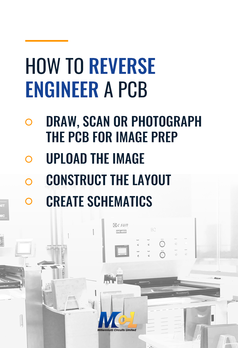
1. Draw, Scan or Photograph the PCB for Image Prep
The first step to reverse engineering a PCB is drawing, scanning or taking a photograph of the PCB. If you take pictures of it, ensure you photograph both sides of the PCB. It’s also crucial to take pictures of it on a dark background. Since PCBs may have holes in them, you don’t want any background visible through these holes, as lighter backgrounds might look like copper. A dark background prevents any confusion about the PCB’s construction.
Another necessary step for properly photographing PCBs is to use a high-quality camera that can capture every detail. Digital cameras or smartphones usually suffice for this step. Additionally, you’ll want to ensure the PCB is well lit. Photographing or scanning images will involve a lengthy process afterward where you’ll need to perform color-switching or image editing. These steps are often required for complex layouts, as photographs and scans can pick up more complicated layouts.
For simpler PCBs, you may be able to draw the layout on a piece of graph paper. If you’re drawing the PCB, ensure you capture the PCB’s exact scale, and use symbols for every component. While manually drawing a PCB can be difficult, it can let you bypass the color-switching and image editing and start on the schematic preparation immediately.
2. Upload the Image
Once you’ve taken the pictures, you can then upload them to your reverse engineering program. Before you upload the imagery, manually crop the image so the photo only shows the PCB. There are multiple programs available online to help you edit any photos or scans and manipulate key PCB features.
For instance, you may want to use GIMP or Inkscape — both platforms are open-source, free graphics editors. Inkscape is a vector graphic editor. Dia is another free, open-source software solution for general-purpose diagramming. You may also want to consider using AutoTrace, a program that converts bitmap to vector graphics.
All these programs can be helpful in the schematic development and layout building processes. Once you complete the schematic development and layout building processes, you may still require CAD software to get more detailed results.
3. Construct the Layout
After uploading your images to your chosen reverse-engineering PCB program, you’ll then need to build a 3D layout of the PCB. A PCB’s layout shows how the system’s electromagnetic field distribution is arranged and how the circuits behave. It also represents other parts of a PCB that can’t be shown in a schematic, such as components, conductive elements, the arrangement of traces and each layer’s planes.
If you’re reverse engineering a simple PCB, you can often just scan a drawing of the PCB and upload it to AutoTrace — or a program like it — to build a layout. This type of program will take the bitmap image and convert it into a vector graphic, helping you obtain the PCB’s schematic quickly.
For a more complex PCB, you’ll have to put your image through many editing steps prior to creating a schematic. Generally, you can expect these steps to take some expertise and require many hours as you attempt to build the layout.
The following are some primary editing steps used on each side of the PCB to build the layout:
- “Paint” holes and solder pads: Before transferring the PCB, you’ll need to “paint” the solder pads and holes to ensure you don’t lose them. You can achieve this by swapping channels, as these can improve the holes’ visibility.
- Remove PCB trackpads: Users who run their PCBs through AutoTrace will need to get rid of any PCB trackpads before using the software. These PCB trackpads can convert to loops in the program, so you should remove them to maintain accuracy.
- Mark free holes: Multilayer boards often have holes or areas on them that don’t connect to anything else or connect to the PCB’s inner layers. You should mark these holes during the editing stage so you can identify them.
- Adjust saturation and layers: To increase visibility on painted PCBs, adjust the saturation and layers.
- Clean tracks: Before converting the PCB imagery in a program like AutoTrace, clean any tracks. If you leave the tracks messy, the resulting schematic can be unclear due to poor conversion. You may also want to smooth an image’s edges to ensure the picture converts cleanly.
- Desaturate and invert image: To desaturate the image, apply grayscale to it. Once you complete this, you’ll invert the image so the PCB’s lines become dark and are displayed on a white background. This desaturation process is crucial to obtaining a more accurate AutoTrace transfer, as it clears out any white or gray colors.
- Repeat process on the other side: To craft a full layout, you’ll need to conduct the above editing steps on the other side of the PCB. If you don’t repeat the processes for the other side of the PCB, you won’t be able to produce the dual-sided schematic needed to reverse engineer a circuit board.
4. Create Schematics
The next step is to derive the PCB’s schematic. When you derive a PCB’s schematic diagram, you can see every circuit and all of the board’s components. The diagram will usually take the form of a 2D CAD assembly drawing. This 2D representation of the schematics helps an engineer see how different components connect and what their functionalities are. All of this information is crucial when you’re attempting to repair or reproduce a PCB.
To create a schematic, you can use a program like AutoTrace or a PCB layout CAD program tool like Target 3001!. This step is often relatively easier than the layout stage, as you’ll have already finished any drawing or photo editing needs.
After creating the schematics, you’ll need to combine both sides of the PCB, arrange the tracks and label the components with symbols. By labeling and arranging tracks, you’ll find it easier to interpret the schematic. If you’re reverse engineering a PCB so you can repair it, you can go through the schematic and use it to troubleshoot the PCB. This troubleshooting process often involves replacing any needed lines and inspecting key components.
With the layout and schematics in hand, you should have a full understanding of how the PCB works.

Choose Millenium Circuits Limited for Your PCB Engineering Solutions
With all the complex requirements that come with reverse engineering PCBs, you may want to turn to PCB experts for assistance with the process. Whether you want to improve on an old PCB design or create something new, Millenium Circuits Limited has you covered.
At MCL, we’re dedicated to producing top-quality PCBs for companies in various industries. We can provide you with almost any kind of PCB you could think of, which helps us meet virtually any of your needs. We can even produce prototype PCBs for times when you need a unique solution for your manufacturing processes. Prototyping PCBs can offer a wide range of benefits for businesses. When you need anything from buried via PCBs to double-sided FR4 circuit boards, we have the answers to your problems.
If you have any questions about reverse engineering or want to know more about our engineering solutions in particular, please contact us. One of our representatives will respond to you as fast as possible to give you the help you’re seeking.
Industrial Technology
- Path to Becoming a Cloud Security Engineer: Skills, Responsibilities, and Certifications
- Tiny PCBs: Pushing the Limits of Compact Circuit Design
- Comprehensive Guide to Auditing PCB Suppliers for Quality and Reliability
- Selecting the Right PCB Manufacturer: A Practical Guide for Quality & Reliability
- Copper PCBs: Enhancing Reliability in PCB Manufacturing
- Master PCB Assembly: Professional Techniques for Reliable Electronics
- Mastering PCB Assembly Cost Estimation: 8 Key Factors
- The Origins of Printed Circuit Boards: A 130-Year Evolution
- Mastering PCB Interference Mitigation: A Professional Guide to Ensuring EMC Compliance
- PCB Recycling 101: Part I – Recovering Gold, Copper, and More Safely