


SMT PCB Design Essentials: Expert Component Layout for Superior Quality
Component layout has to meet the requirement of the whole machine electric properties & mechanical structure and the requirement of SMT production craft. Since it's difficult to overcome product quality problem caused by design, PCB designers have to understand the basic SMT craft attributes and implement component layout design according to different craft demands. Excellent design can reduce the soldering defects to the minimum.
Overall Component Layout Design
• Component layout on PCB should be flat and even. Components with big mass will suffer from high thermal capacity in the process of reflow soldering so that locally low temperature is caused by over-integrity layout, leading to false soldering.
• Maintenance space should be left around large components (the left size should be compatible with SMD rework device heating tip).
• High-frequency components should be positioned evenly at the edge of PCB or the vent position inside the machine.
• In the process of single-mixed assembly, mounted and plug-in components should be positioned on Side A.
• In the process of double-side reflow mixed assembly, large mounted and plug-in components should be positioned on Side A and components on Side A and B should be staggered.
• In the process of Side A reflow soldering and B wave soldering mixed assembly, large mounted and plug-in components should be positioned on Side A (reflow soldering side) while rectangular and cylindrical chip components that are suitable for wave soldering, SOT and relatively small SOP (pin number less than 28 and spacing between pins at least 1mm) are positioned on Side B. Components with pins around mustn't be positioned on wave soldering side, such as QFP, PLCC etc.
• Component package on wave soldering side has to stand the temperature of over 260°C and be hermetic.
• Valuable components can neither be positioned at the four corners or edge of PCB nor near connector, assembly hole, slot, cutting groove, nick or corner. The places mentioned above belong to areas with high stress, leading to crack of soldering points and components.
Component Layout Direction
• Component layout direction with reflow soldering craft
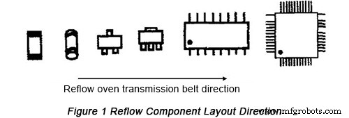
For PCB with big size, the long edge of PCB should be parallel with the reflow oven transmission belt direction so as to make the temperature of both sides of PCB compatible with each other. Therefore, for PCB whose size is more than 200mm, the following requirement must be met:
a. Long axis of chip component with two ends is vertical to PCB'S long edge and the long axis of SMD component parallel with PCB's long edge.
b. The directions of double-layer assembly PCB should be the same.
• Component layout direction with wave soldering craft
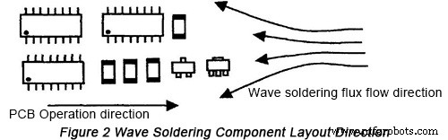
a. In order to make the corresponding two ends of components connected with wave soldering flux simultaneously, the long axis of chip component should be vertical to the direction of transmission belt of wave soldering machine and the long axis of SMD component should be parallel with the transmission belt direction of wave soldering machine.
b. In order to avoid shadow effect, the ends of components with the same size should be positioned in one line parallel with the transmission belt of wave soldering. Components with different sizes should be positioned along different directions. Components with small size should be placed before big components. It should be avoided that components possibly block the soldering ends and soldering pins. When the requirements concerning component layout fail to be met, the spacing of 3mm to 5mm should be left between components.
c. Compatibility of component characteristic direction
It should include electrolytic capacitor polarity, anode of diode, single pin end of triode and the pin I of IC.
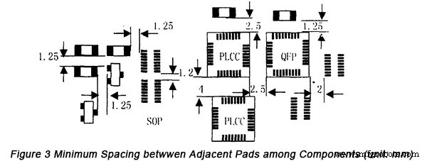
The Minimum Spacing between Adjacent Pads among Components
Besides that the safe spacing between pads shouldn't be connected for a short distance, the maintainability of vulnerable components should be also considered. Generally speaking, the assembly density should meet the following requirements:
• The spacing between chip components, SOTs, SOIC and chip components is 1.25mm.
• The spacing between SOICs, SOIC and QFP is 2mm.
• The spacing between PLCC and chip components, SOIC, QFP is 2.5mm.
• The spacing between PLCCs is 4mm.
• For mixed assembly, the distance between plug-in components and chip component pad is 1.5mm.
• In the process of PLCC socket design, sufficient space for PLCC socket should be maintained in advance.
The specific spacing between adjacent pads among components is displayed in Figure 3 below.
High-quality SMT PCB Manufacturing Service At lower Cost
With over ten years' experience in SMT PCB fabrication and assembly, PCBCart is fully capable of bringing your PCB design into real circuit boards with the expectant performance, we are very good at meeting customers' specific requirements on lead time and budget. If you happen to have a design ready for prototype or production run, why not reach us for a free quotation first? Then you may decide whether to go on with us.
Helpful Resources
• Can't-Miss Engineer-Friendly PCB Layout Guidelines
• Layout and Tracing Rules for Box Build Assembly
• Design Requirement of SMT PCBs Part One: Bonding Pad Design of Some Ordinary Components
• Design Requirement of SMT PCBs Part Two: Settings of Pad-Trace Connection, Thru-Holes, Test Point, Solder Mask and Silkscreen
• Design Requirement of SMT PCBs Part Four: Mark
• Full Feature PCB Manufacturing Service from PCBCart - Multiple Value-added options
• Advanced PCB Assembly Service from PCBCart - Start from 1 piece
Industrial Technology
- Optimizing SMT Component Placement on PCBs for Reliability
- Choosing the Right PCB Layout Software: Expert Comparison & Recommendations
- Essential PCB Layout Strategies for Reliability and Cost Efficiency
- SMT PCB Design Essentials: Pad-Trace Connections, Thru-Holes, Test Points, Solder Mask & Silkscreen Guidelines
- SMT PCB Design: Bonding Pad Guidelines for Standard Components – Part 1
- SMT PCB Design Guidelines: Part 4 – Marking Standards for Accurate Fabrication
- Three Key Design Strategies for Optimal EMC in Laptop PCBs
- Optimizing PCB Assembly: Stencil Design Guidelines for QFN Components
- Essential DFMA Guidelines for Efficient PCB Design & Production – Part I
- Essential Design Guidelines for PCB Manufacturing & Assembly – Part II