


Semiconductor Innovations Powering Faster, Safer, and High‑Efficiency EV Chargers
Semiconductor Innovations Powering Faster, Safer, and High‑Efficiency EV Chargers
As electric‑vehicle fleets grow, the demand for charging infrastructure that delivers power quickly, reliably, and with minimal losses has never been higher. Modern EVs feature larger battery packs that require fast DC‑charging solutions. A 150‑ or 200‑kW station can bring an EV to 80 %—enough for roughly 250 km—in about 30 minutes, while the latest Combined Charging System (CCS) and Charge de Move standards push the ceiling to 400 kW.
Key semiconductor breakthroughs—high‑voltage switches, high‑frequency converters, and multi‑level power stages—are making this level of performance achievable. Below we examine the technology enablers that bring speed, safety, and efficiency together.
- High‑Voltage Switches – IGBTs and SiC devices now support bus voltages of 800 V or even 1,000 V, driving up power density but also demanding stronger isolation.
- High‑Frequency Converters – Switching rates from hundreds of kHz up to a few MHz shrink magnetic components, cut cost, and improve density. This requires ultra‑wide‑bandwidth current/voltage sensing.
- Multi‑Level Power Stages – To squeeze the most efficiency from a high‑voltage system, complex multi‑level topologies rely on isolated gate drivers that keep switching losses low while offering robust protection.
Isolation Technologies
Safety compliance is paramount for chargers that sit directly on the utility grid. Isolation protects operators, protects control electronics from high‑voltage transients, and eliminates ground‑loop issues. In high‑voltage DC‑link systems, isolation levels range from functional (operational) to reinforced (double‑insulation) depending on the operating voltage.
Three primary isolation methods are used in modern semiconductors:
- Optical Isolation – Uses LED‑driven photodiodes. Offers high isolation, low cost, but suffers from long propagation times and limited noise immunity.
- Magnetic Isolation – Employs transformer coupling. Provides high isolation at high frequencies but introduces electromagnetic noise and temperature‑dependent insulation loss.
- Capacitive Isolation – Transmits energy through a changing electric field. It delivers high speed, excellent common‑mode transient immunity (CMTI), and superior temperature stability—ideal for gate drivers and amplifiers.
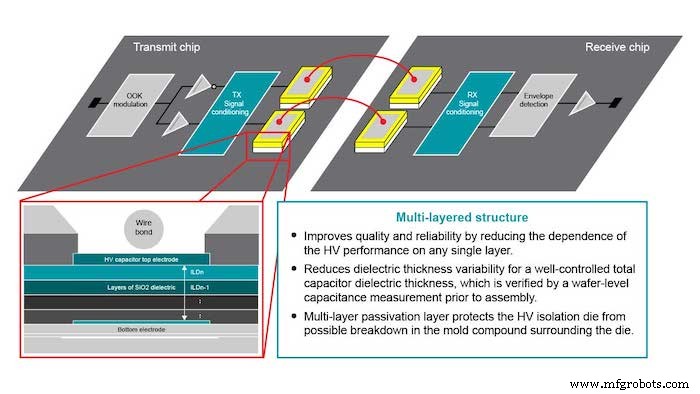
Figure 1. Capacitive isolation
High‑Bandwidth Current and Voltage Sensing
Accurate sensing is critical for monitoring, protection, and control in every stage of the charger’s power flow—from power‑factor correction to DC‑DC conversion. Figure 2 illustrates the key sensing locations.
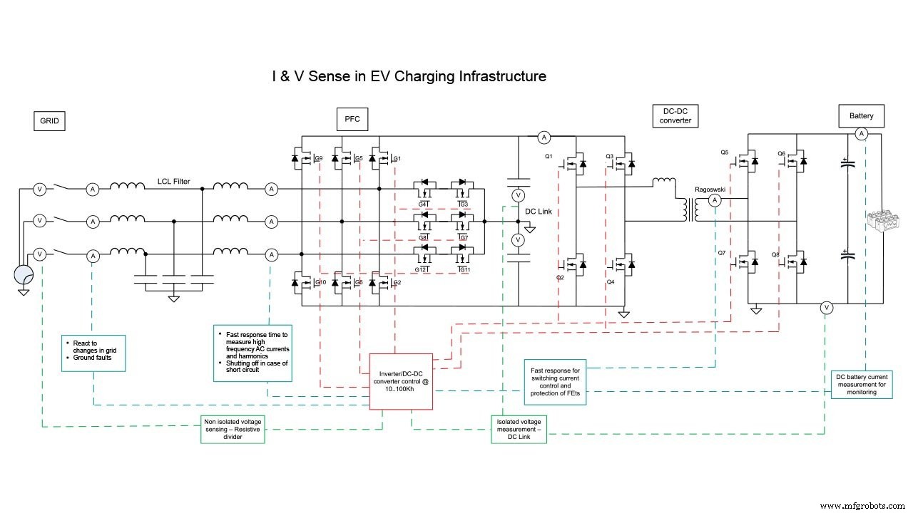
Figure 2. Block diagram of an EV charging station
SiC and GaN switches enable operation at frequencies up to a few megahertz, demanding fast, linear, and temperature‑stable sensors. Two sensing paradigms dominate:
- Direct Sensing – Shunt resistors (50 mV or 250 mV drop) coupled to isolated amplifiers or sigma‑delta modulators. Shunt sensing offers superior DC accuracy and linearity across the full range, reinforced isolation up to 5 kV, and a smaller footprint than Hall‑effect sensors.
- Indirect Sensing – Hall‑effect sensors detect magnetic fields around the conductor. Open‑loop sensors reach 1 MHz bandwidth; closed‑loop sensors (350 kHz) provide better precision at higher cost. Hall sensors excel in short‑circuit detection, crucial for SiC switches that can tolerate only 1–3 µs before a fault.
Isolated Gate Drivers
Gate drivers bridge the pulse‑width modulator and the high‑power switch. They must source and sink peak currents at gigahertz rates, keep propagation delays low, and match drive times for parallel MOSFETs. For high‑voltage applications, reinforced isolation protects against common‑mode transients (CMTI > 100 V/ns) and leakage.
Key features for next‑generation chargers include:
- Wide‑range voltage flexibility and compatibility with IGBTs, SiC, and GaN devices.
- Robustness to EMI and high temperatures.
- Integrated DESAT pins and active Miller clamps for rapid short‑circuit detection and prevention of false turn‑on.
- Low on‑resistance and low output capacitance to boost power density by up to 33 %—particularly valuable for portable DC fast chargers that rely on natural convection cooling.
Resonant architectures, combined with zero‑voltage and zero‑current switching, further suppress switching losses, enhancing overall efficiency.
Conclusion
As charger power and voltage levels climb, the need for high‑density, reliable, and safe power converters intensifies. Manufacturers are moving from conventional IGBTs to SiC and GaN devices, operating at hundreds of kHz to megahertz frequencies. Coupled with high‑bandwidth sensors and advanced isolated gate drivers, these technologies make it realistic to charge an EV to full range in the time it takes for a quick coffee break.
Co‑authored by Harish Ramakrishnan, Systems Engineer, Texas Instruments.
Industry Articles provide partners with technical insights. All viewpoints reflect the authors, not All About Circuits.
Industrial Technology
- Smart Manufacturing 2021: 10 Emerging Trends Reshaping Production
- Industrial Technology: A New Era of Efficiency and Growth
- TI Introduces Ultra‑Compact, High‑Efficiency BQ25790/BQ25792 Buck‑Boost Battery Chargers
- How Machine Vision Enhances Food Safety & Reduces Recall Costs for Manufacturers
- Why Modern Manufacturers Must Embrace Technological Innovation
- Why Logistics Tech Implementations Fail—and How to Overcome Them
- Same-Day Ship-From-Store: 5 Expert Tips for Lightning-Fast Delivery
- Quick & Accurate Brake Horsepower Calculation – Simple Formula & Step‑by‑Step Guide
- Ericsson's 5G Solutions Drive Manufacturing Digital Transformation
- Top 10 Military Technology Trends Shaping 2022