


Mastering PCB Design: Overcoming Common Challenges
Designing a reliable printed circuit board (PCB) is foundational for building high‑performance, cost‑effective prototypes—especially in embedded systems where hardware constraints are tightly coupled with software complexity.
From a schematic, engineers can simulate signals, generate Gerber and drill files, and validate the layout before manufacturing. Selecting the right PCB design tool is therefore critical; the ideal solution must be intuitive, feature‑rich, stable, and backed by a comprehensive component library to support diverse projects.
Hardware Considerations
In IoT deployments, seamless integration of conductive and non‑conductive materials dictates both performance and reliability. As device footprints shrink, the heat generated by dense components becomes a dominant design factor. Thermal management—through careful layout, copper pour design, and material choice—ensures predictable temperature response and component longevity.
Protection is achieved by insulating copper traces and isolating high‑voltage areas. FR‑4 remains the industry standard for its mechanical robustness, high‑frequency fidelity, excellent heat resistance, and low moisture absorption. It is widely adopted in high‑end, industrial, and military boards, and even supports ultra‑high vacuum (UHV) environments.
However, traditional FR‑4 can suffer from inclusions, streaks, and glass‑fiber deformation during manufacturing, which degrade dielectric strength and trace performance. Modern epoxy‑glass composites address these issues, offering superior consistency and reliability.
Alternative substrates such as polyimide/fiberglass provide higher temperature tolerance and rigidity, while Kapton offers flexibility and low weight—ideal for displays, keyboards, and wearable devices. Key selection criteria include coefficient of thermal expansion (CTE), glass‑transition temperature (Tg), thermal conductivity, and mechanical rigidity.
Military and aerospace boards must adhere to strict layout specifications and achieve 100 % design‑for‑test (DFT) coverage. The MIL‑STD‑883 standard prescribes comprehensive mechanical and electrical testing, manufacturing protocols, and training requirements to guarantee uniform quality across critical applications.
Automotive PCBs face additional constraints, such as compliance with AEC‑Q100 mechanical and electronic testing for packaged ICs. Crosstalk and electromagnetic interference (EMI) can jeopardize vehicle safety; designers must maintain minimum spacing between signal and power traces. Advanced design‑automation tools can flag violations of interference limits and thermal budgets, enabling rapid iteration without compromising system integrity.
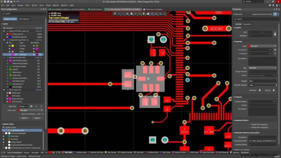
Figure 1: Altium Designer (Image: Altium)
Signal quality is further challenged by vehicle‑generated noise, which couples through the chassis and induces unwanted currents. Voltage spikes from the ignition system can push components beyond their tolerance limits, underscoring the importance of robust layout and shielding practices.
Embedded
- Optimizing Grounded Coplanar Waveguide RF Feedlines for Enhanced Wi‑Fi Performance
- Overcoming Design Challenges in Precision DC Energy Metering
- Choosing the Right PCB Layout Software: Expert Comparison & Recommendations
- Essential PCB Layout Strategies for Reliability and Cost Efficiency
- Master PCB Design Quickly with Ultiboard: A Comprehensive Tutorial
- Master Pulsonix PCB Design: A Comprehensive Tutorial for Windows Users
- Master PADS PCB Design: Advanced Features & Tutorials
- Proven High‑Speed PCB Layout Tips for Reliable Designs
- Expert PCB Thermal Design: Practical Tips for Heat Management
- Common PCB Design Challenges and How to Avoid Them