


Advanced BGA Inspection Techniques for Reliable Electronics
Ball Grid Array Inspection Techniques
The constant progress of technology has moved electronics toward small, lightweight products. To keep up with these consumer desires, surface-mount technology (SMT) was introduced. However, increased demand for these products also required the development of high-density technologies that could be quickly assembled. This push led to the development of ball grid array (BGA) technology.
BGA and similar devices have quickly become a standard element in modern printed circuit board (PCB) design. However, these devices are notoriously difficult to inspect after assembly. In this article, we’ll discuss the challenges of BGA inspection, inspection techniques used in BGA quality control and ways to avoid common BGA defects before assembly.
What Is a Ball Grid Array Inspection?
A ball grid array is a surface-mount package for integrated circuits that is used to mount devices. The BGA’s bottom surface is covered in pins arranged in a grid pattern, hence the technology’s name. Instead of being wire pins, these connections are made with pads with balls of solder. These connections need to be carefully soldered due to their location underneath the package.
Once the solder connections are complete, however, they are no longer visible to the casual observer. Because they are not visible, more advanced inspection techniques are required to ensure their quality. This is where BGA inspection plays a vital role.
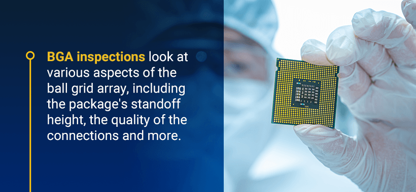
BGA inspection is a process where the connections between a chip and a PCB are analyzed to ensure quality. BGA inspections look at various aspects of the ball grid array, including the package’s standoff height, the quality of the connections and more. In BGA inspections, unassisted visual inspection is extremely limited, so other techniques are required to get a detailed look at the connections.
These analysis methods include electrical testing, assisted optical inspection and X-ray inspection. The components of these techniques will be discussed in greater detail further along in this article.
Why Is Inspection Important?
BGA inspection is notoriously difficult for one reason — the solder joints are located beneath the BGA package. Because of this feature’s positioning, it can be challenging to get a good view of the BGA for inspection. Despite this difficulty, inspection is essential for BGAs for several reasons, including:
- Soldering difficulty: Soldering BGA components is tricky, as it requires sufficient heat to be applied to the array so all balls in the grid melt sufficiently to make solder joints. Both the density of connections and the difficulty of soldering mean there is a high likelihood of a defect occurring. Inspections help experts catch these defects so they can avoid sending out faulty parts.
- Unreliable electrical tests: Electrical tests run a current through the PCB to ensure it is electrically sound. However, this type of test can only judge whether the current is on or off when the BGA components are connected. These tests are not reliable as they can only find a handful of defect types and cannot pinpoint the locations of any defects they find. Comprehensive inspections that combine this method with other techniques can create a more complete overview of errors and their locations.
- Material reuse: If a BGA is found to have a solder defect, it can be removed using a rework station and replaced or refurbished for reuse. The inspection process identifies defects early on so materials can be saved in this way, which reduces material waste.
- Quality control: BGA SMT assembly relies on quality physical connections, so BGA quality control must include a detailed inspection of these connections. Inspections can also identify common defects and patterns. These are important, as repeated defects may indicate issues with the manufacturing and assembly process or even the PCB product design.
- Cost reduction: Thorough inspection processes minimize the number of defects that pass on to the next stage of production. Defects that pass inspection may get caught further along in the production process, making rework more costly. The later the defect is caught, the more expensive it will be for your company. That is why early prevention and resolution is crucial.
Because of the importance of inspection, inspection teams must utilize thorough and effective tools and techniques in the process. That way, these teams can catch all issues and pinpoint their locations and causes before they become bigger and costlier problems.
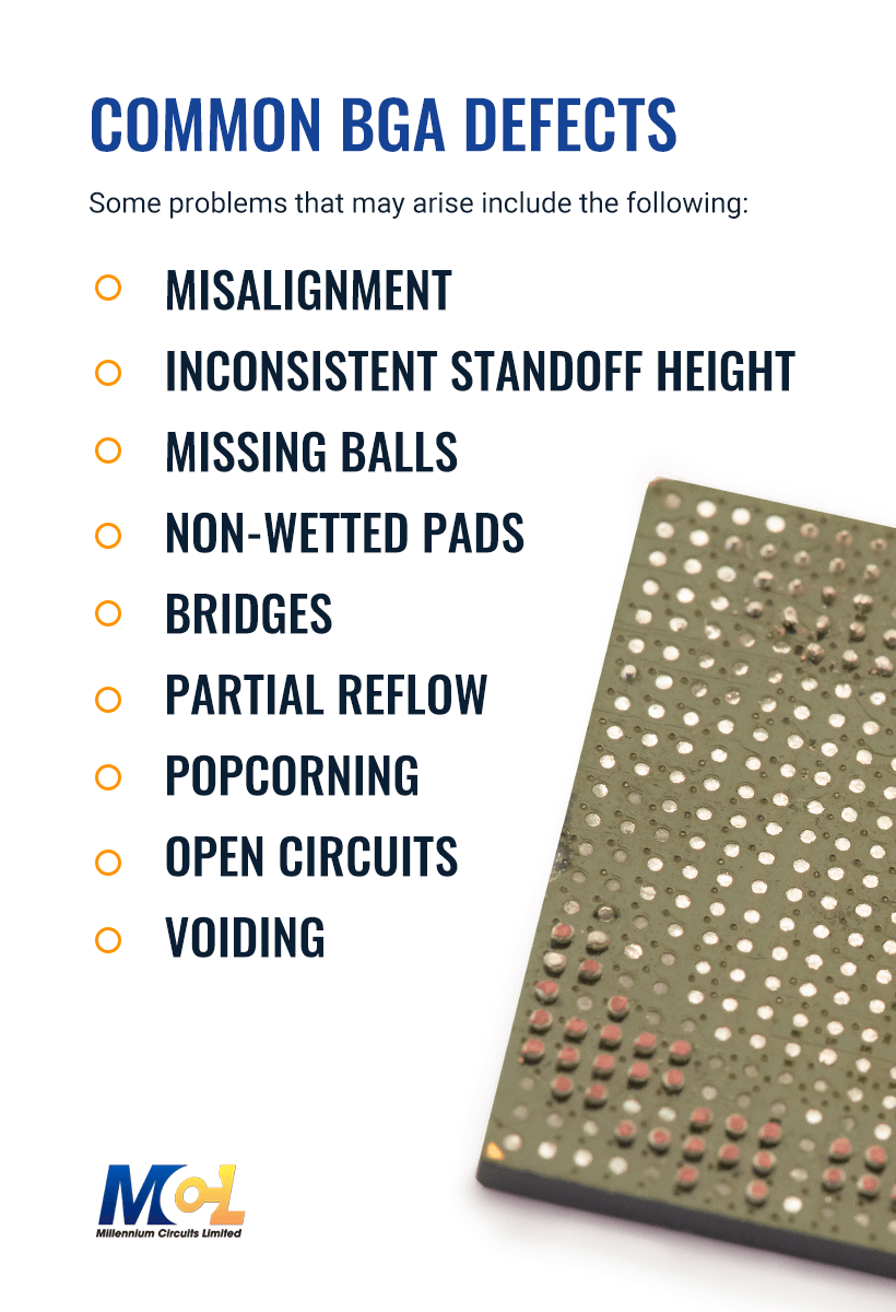
Common BGA Defects
Due to the BGA’s complexity, many potential defects can occur during the soldering process for a BGA. Some problems that may arise include the following:
- Misalignment: Misalignment happens when the PCB and BGA are offset during reflow and connect at incorrect points. This is one of the most common issues that occurs during BGA assembly.
- Inconsistent standoff height: BGAs are set on top of PCBs, and improper soldering can result in the BGA setting at a crooked angle on the surface of the PCB. This asymmetric standoff height can compromise the security of connections.
- Missing balls: If balls are missing from the BGA when it is attached to the PCB, essential connection points may be missing from the assembly.
- Non-wetted pads: In some cases, reflowed solder paste may not wet the pad correctly. This may result from incomplete reflow or leftover solder resist from previous steps in the production process.
- Bridges: Bridges occur when extra solder paste is left between paste deposits. Bridges between connection points often result in shorts.
- Partial reflow: In some cases, the reflow may not completely cover the board. This often occurs because of insufficient solder reflow, human error or mechanical malfunctions.
- Popcorning: Popcorning occurs when balls merge together during the soldering process. This is a common problem for BGA and, like bridges, results in shorts.
- Open circuits: Open circuits occur when solder fails to wet the PCB pad and climbs onto solder balls and onto the component surface. While an electrical test can identify this as a problem on a board, it cannot identify the cause of the issue.
- Voiding: Voiding occurs when flow stops short of a solder connection. This is a common problem in collapsible BGA components.
These issues can all be fatal errors for the final product, so catching them with quality inspection techniques and technologies is a necessity. Fortunately, modern inspection techniques have advanced to a point where most of these defects can be identified using one or more inspection methods. However, it is also essential to avoid these defects wherever possible before assembly.
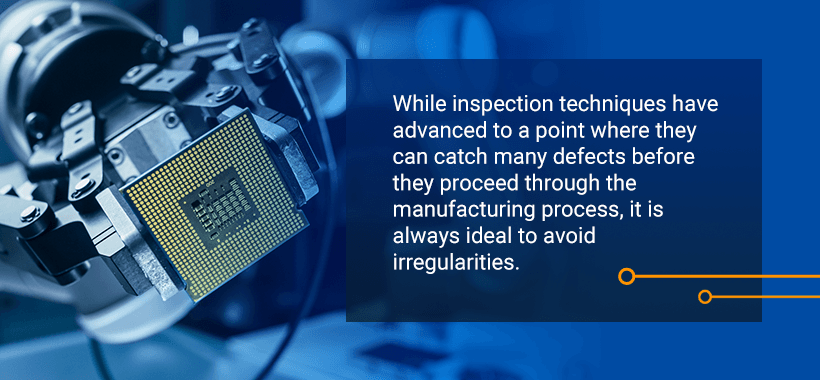
Design Considerations to Avoid BGA Defects
While inspection techniques have advanced to a point where they can catch many defects before they proceed through the manufacturing process, it is always ideal to avoid irregularities. This requires careful planning from the design team. To maximize the chances of achieving successfully soldered joints on a BGA, design teams should consider the following in the PCB layout:
- BGA footprints: PCB designers need to make sure they have the correct footprint pattern for the BGA device they wish to use. Ensure the footprint is correct and take care to design the PCB footprint pad precisely to avoid shorts and solder issues during assembly.
- Thermal management: The PCB layout must consider thermal mass. Grouping BGAs closely together can cause a thermal imbalance between highly populated and less populated parts of the board. For example, applying enough heat to properly solder closely grouped BGAs may result in burns in less populated areas. Conversely, applying sufficient heat to avoid burning less populated areas may result in voids in the BGAs.
- Via placement: Vias or through-holes are common features of PCBs, but the placement of vias can affect the behavior of solder in the BGA assembly process. Vias adjacent to a BGA pad can result in excess solder running from the pad to the via, causing a short. To avoid this, tent any vias adjacent to a BGA pad with solder mask.
On top of these design considerations, you should also take care to develop and verify a proper reflow profile before assembly. This involves using a profiler to measure and log the temperature range at the BGA ball/pad junction when the board passes through the reflow oven. This can be done with scrap bare PCBs and BGA parts. This data can be used to ensure the reflow profile for the paste and the thermal profile of the PCB is correct, plus identify any design issues before assembly.
Inspection Techniques for Ball Grid Array
Avoiding defects is the goal, but BGA inspection is always necessary to analyze the connections between a BGA and PCB. Because it is almost impossible to see the solder joints through direct visual observation, this analysis is accomplished using various inspection techniques and tools. These tools and techniques have evolved over the years to be dependable and user-friendly. While these tools cannot be used individually to cover all aspects of inspection, they can provide a comprehensive view of the BGA when combined.
Inspection tools and techniques are often organized into the following categories:
1. Electrical Testing
Electrical testing of BGAs is another inspection process that tests the board’s electrical properties. This is different from mechanical testing, which is a destructive process that subjects the BGA to shock and shear tests to evaluate the quality of solder joints under stress.
Electrical testing runs a current through a BGA to analyze the electrical stability of the board. The test determines whether the current is on or off after the BGA component is connected. This type of test is useful for identifying if there are any electrical problems such as shorts or opens. However, as previously discussed, electrical tests can only identify the presence of these defects — they cannot be used to locate where a defect is on a BGA.
While electrical testing is an important step in the inspection process, it is difficult to pick up test points under BGA components. It is also difficult to meet assessment requirements with electrical tests alone. Instead, electrical tests are often used in combination with other test techniques to identify issues in a ball grid array inspection.
2. Optical or Visual Inspection
Optical inspection, also referred to as visual inspection, is the use of optics technology to view a BGA and its connections. This technique historically used the naked eye or microscopes, which delivered limited results. However, introducing the endoscope has proven particularly valuable for this inspection technique.
The endoscope was originally designed for medical applications, but the technology’s ability to visually inspect tiny objects in confined areas makes it ideal for BGAs. The technology involves using a camera with a high magnification lens and a connected monitor to gain close-up images of an inspection area. This technology is often paired with visualization software for advanced image capture and measurement.
Visual inspection with an endoscope allows technicians to look at the outer row of connections between a BGA and PCB — with good lighting, technicians can also view some interior rows. This optical technique helps identify and assess the overall quality of a solder joint, including the joint’s shape, surface texture and appearance, which can all indicate different defects.
Optical inspection can also identify shorts, opens, debris and cold solder and is essential for assessing rework, as it can identify proper reflow coverage. However, the visual capability of this inspection technique is limited and does not allow for detailed analysis of internal connections.
One final note about endoscopes is that they are a highly versatile piece of inspection equipment. Endoscopes can be used to inspect BGA solder joints as well as various surface-mount and through-hole mount assemblies that can be difficult to analyze through normal methods.
3. X-Ray Inspection
The most advanced inspection method for BGAs is X-ray inspection. X-rays work by emitting X-ray energy from an X-ray tube onto the board. X-rays pass through the board at differing amounts, with more X-rays trapped in dense areas such as solder joints. The X-rays are then collected at a detector, which translates them into visible light and generates an image.
In this image, solder joints are darker than their surroundings, allowing the viewer to see solder patterns. The resulting image will show a uniform grid of identical dark circles in an ideal board, the circles being the solder joints.
The X-ray test results in an image where the ball grid and solder patterns are easily seen and inspected from a top-down angle. More advanced X-ray inspection technology features a tilt function, which can analyze the shape of solder joints from different angles. These images are particularly useful for seeing variations in solder patterns and shapes, making this a good technology for identifying solder bridges, popcorning, excess solder and similar defects. This technology, however, is not good at detecting opens.
Like endoscopes, X-ray inspection technology can be used in various applications outside of BGA inspection. Some examples include via and through-hole inspection, surface-mount defect analysis and unleaded solder inspection.

Contact Millennium Circuits
When used in combination with one another, effective and thorough ball grid array inspection techniques can greatly reduce the number of defects that pass the inspection stage. By reducing the amount of defects that move on in the production process, businesses can decrease the occurrence of costly rework and recalls. However, it’s always ideal to avoid BGA defects through quality design. If you have any questions about BGAs, inspection techniques and ways to avoid BGA defects, contact the experts at Millennium Circuits for more details.
Millennium Circuits Limited (MCL) is an industry-leading PCB supplier based in central Pennsylvania. Our goal is to give you the best PCBs at the best prices and provide you with the PCB knowledge you need to stand out from your competitors. With over a decade of dedicated service, multiple awards and over 400 customers worldwide, MCL is a printed circuit board company you can trust.
At MCL, we take immense pride in helping our customers achieve a greater understanding of electronics and learn how to ensure maximum quality and competitiveness within the market. We’re happy to provide you with any information you need to make informed decisions about your electronic components. Reach out to MCL today to learn more about BGA quality control and inspection.
Industrial Technology
- Understanding Electron Tubes: Components and Functionality
- Expert Guide to JFET Biasing Techniques: Achieve Stable, High‑Performance Circuits
- Expert Guide to Biasing Techniques for IGFETs
- Advanced Heat Dissipation Techniques for Reliable PCB Performance
- BGA vs. LGA: Key Differences in IC Grid Array Packaging
- Top 6 Benefits of Ball Grid Array (BGA) Packaging for PCBs
- Ball Grid Array (BGA) Explained: A Complete Guide to High-Density PCB Technology
- Essential PCB Inspection Techniques for Quality Assurance
- Ball Grid Array (BGA): Key Advantages and Drawbacks Explained
- Ball Grid Array (BGA): Key Acceptance Criteria and Advanced Inspection Techniques