


Expert Guide: Troubleshooting Wave Soldering Issues on PCBs
Jump To: What is Wave Soldering? | Wave Soldering Defects and Remedies
What Is Wave Soldering?
Wave soldering is a type of soldering process used during the bulk manufacture of printed circuit boards, or PCB. The wave soldering process allows manufacturers to quickly and reliably solder large printed circuit boards. The process gets its name from the wave of solder each board gets passed over. Using a wave of solder as opposed to individual solder points produces solder joints that are mechanically and electrically reliable.
The wave soldering process is effective for both the conventional through-hole method of PCB assembly and also the newer surface-mount method.
So what’s in a wave solder machine, and how does the process work?
At its core, a standard wave solder machine starts with one component: a heated tank of solder that is maintained at the required temperature for the specific soldering process that is taking place. Inside the tank, the technician sets up a wave of solder, then passes each PCB through the tank, so the top of the wave of solder just makes contact with the bottom of the PCB.
Designers need to be aware of two major issues when it comes to designing printed circuit boards that are going to be wave soldered.
- Pad spacing: If the pads that need to be soldered are too close together, liquid solder can flow between them. Short-circuiting of not only the two connected pads, but possibly the entire PCB, is the result.
- Solder resist: Having a layer of solder resist on the printed circuit board isn’t as much of an issue as it was in the past, as a solder resist layer is in the blueprint as standard practice. Still, double-checking that a solder mask or solder resist layer is part of your PCB’s blueprint is always a good thing to do, and helps prevent unfortunate accidents.
Once the board to be soldered has been checked for pad spacing and a layer of solder resist, it’s time to apply flux. Flux helps ensure the areas of the board that need to be soldered are clean and free of oxidation. There are two different ways to apply flux, depending on the circumstances.
- Spray flux, which can be applied as a fine mist and followed up with a jet of compressed air to remove any excess.
- Foam flux, which is applied to the board from a tank of regular flux. A plastic cylinder with tiny holes is submerged in the tank of flux. Once the cylinder has been well and truly submerged, a metal chimney can be fitted over the top of it. Air can then be forced through the cylinder to get foam to rise out through the chimney. The bottom of the PCB can then be coated in this foam flux.
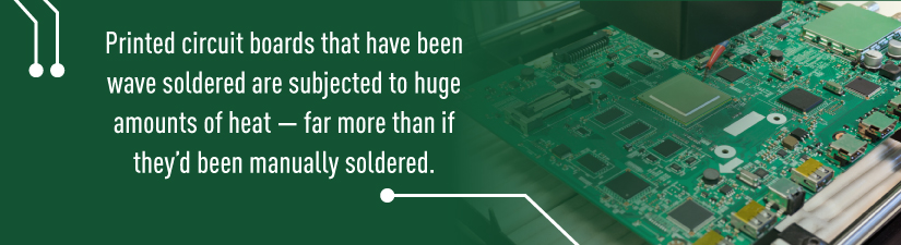
Once you’ve treated the underside of the board with flux, it’s time to preheat the board. Because of the way solder is applied as part of the wave soldering process, printed circuit boards that have been wave soldered are subjected to huge amounts of heat — far more than if they’d been manually soldered. Without preheating, circuit boards can end up with all different types of soldering defects — all due to thermal shock.
To help minimize the chances of thermal shock, boards that need to be wave soldered must slowly be heated to the required temperature.
What are some of the defects that can happen to wave-soldered boards if they’re not preheated?
Wave Soldering Defects and Remedies
Just because there’s machinery involved in the wave-soldering process does not mean it is any less prone to errors than soldering each joint by hand. Whether you’re using a solder tank or a hand iron, you need to treat soldering like the precise science it is, carefully controlling where and what you solder.
Otherwise, you’ll up with any of several soldering defects like the ones listed below:
- Insufficient Hole Fill
Insufficient hole fill is a problem that occurs on printed circuit boards with pre-drilled holes for components to be mounted onto the board. Essentially, insufficient hole fill occurs when an inadequate amount of solder has filled the holes drilled for the components, meaning solder won’t stick to the circuit board once it cools. There are several reasons for insufficient hole fill:
- The flux was applied incorrectly and did not penetrate through the board, meaning the solder was not activated and could not bind the components properly.
- The temperature of the top side of the board isn’t high enough to turn solder molten so it can rise through the holes.
- There was not enough of the board in the wave of the solder. If not enough of the board makes contact with the wave, too little solder is pushed up into the through-holes.
The best way to fix these issues is to run through another series of pre-solder checks. Check the type of flux you’re using, and make sure there’s a sufficient volume of it to cover the entire PCB. This step will also help with the second problem: insufficient pre-heat.
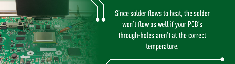
Since solder flows to heat, the solder won’t flow as well if your PCB’s through-holes aren’t at the correct temperature. While the “right” temperature depends on your company’s operating standards, the general rule of thumb is between 300 and 340 degrees Fahrenheit, or roughly 150 to 170 degrees Celsius.
The whole assembly needs to reach this temperature before the board makes contact with the wave. If you’re not sure whether your through-holes are reaching the correct temperature, take a profile of the wave-solder process — it should look either exactly alike or very similar to your board’s reflow processes.
While you’re taking a profile of the wave-solder process, you can also check your board height — that is, how much of the board is exposed to the wave at any one time. Try to have at least half the board thickness running in the solder wave at any one time, which will allow the hydrostatic pressure of the wave to push the solder up into the through-hole.
- Lifted Components
Lifted components, also known as tombstones, are components that have elevated from the board during the soldering process. There are several common causes of tombstones, including:
- Incorrect lead lengths, which can cause components to lift from the board when they enter the solder bath.
- Attempting to perform wave soldering on a flexible PCB, which will bend while the rest of the components stay flat, causing them to lift off the board.
- Using components with varying requirements for solder type and temperature.
To fix the incorrect lead lengths, look at what leads you’re using. If your leads are too long, hitting the solder bath can push them out of the through-hole. To fix this, you can increase the in-wave immersion time, which should lessen the thermal demand on the leads and allow them to settle.
To correct flexing of the PCB or other flex-related issues, double-check what kind of PCB you’re using and what its thermal tolerances are. Board flexing is common on large connectors and on large IC packages or sockets. PCBs that flex from the get-go, such as plastic, should not be wave-soldered, as the wave of solder can cause the plastic to bend and lift the components away from the board.
Finally, once you’ve checked the thermal tolerances of your board, check the thermal tolerances of all your components. Components that have different temperature demands or lead solderability temperatures can also lift on contact with the wave, as some components solder down, while excess heat pushes others away. Make sure all the components you’re using have the same requirements, which should help prevent those sorts of issues.
- Excessive Solder
Excessive solder is the result of your board taking on a buildup of solder when passing through a wave-solder tank. While this still ends up making an electrical connection between the board and the component in question, it will be hard for you or whoever else is looking at the board to tell exactly what’s going on inside the solder itself.
There can be several reasons you might have too much solder on your connections:
- Having the same types of components face different directions
- Using incorrect lead lengths when it comes to your design processes
- Running your conveyor belt too fast
The first cause is an easy enough fix. Make sure all your components of one single type — e.g., all your batteries — face the same way when they go into the wave tank. So, if one component is facing “away” from the tank when it goes in, all the other components of that type should be facing that way, too.
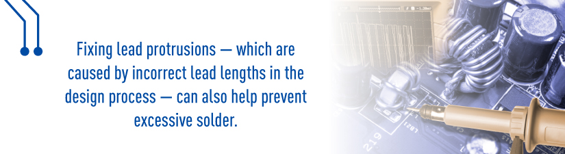
Fixing lead protrusions — which are caused by incorrect lead lengths in the design process — can also help prevent excessive solder. If the lead is too long, solder can pool against it and become excessive. To solve this, decide on a lead length that does not extend too far beyond your pad surfaces. For example, NASA uses a lead length of 2.29 mm — just long enough to stick past the pad for soldering.
If your components are all facing the same way and your solder lengths are precise, you might need to slow your conveyor belt down. A conveyor belt that goes too fast may end up dumping wave after wave of solder on your board’s components as they pass through the solder tank. The easiest fix for this issue is to talk to your project manager about acceptable conveyor belt speeds.
- Solder Balling
Solder balling can occur when small bits of solder re-attach themselves to the PCB — specifically near the leads — as it goes through the wave soldering process. Common causes of solder balling can include:
- The temperature of the solder in the tank is too high.
- Solder is falling back into the wave as it separates from the board, which can cause that excess solder to splash back onto the board.
- Gases released by heated flux can cause liquid solder to get spit back onto the board.
The best way to fix general solder balling problems is in the design of the PCB itself. When it comes time to pick out the solder mask you use in your PCB design, try to find one that has the least chance of allowing solder to adhere to it in the first place. By choosing the best solder mask for your design, you can help make your board design more robust.
Solder balls caused by gases from heated flux usually stem from an excessive backflow in the air around your wave solder tank, or a drop in the nitrogen present in the environment. Check how much air is flowing into the solder tank, as well as the amount of nitrogen present in your solder tank’s environment. Keeping a careful eye on both of these will help alleviate solder ball issues caused by bounce-back from heated flux.
There are several reasons solder might fall back into the wave: whether there’s volatile material still in the flux, how high the solder wave is, etc. The best way to get a bead on the root of the problem is to run your solder wave with a white card over the top of the wave, but without any boards processing. Run the same test with a couple of test boards going through the wave, and compare the results.
- Solder Flags
Solder flags are small protrusions of solder that poke out from the ends of your leads. Even though they will still allow you to form a proper electrical connection with the other components on the board, they indicate both improper flux application and issues with how the solder is draining from your board.
Common causes for solder flags include:
- Slow drainage of the solder from the wave solder machine, leaving an excessive amount of solder on the lead, which will “flag” out to one side as it drains.
- Trails of solder that look like whiskers — commonly the result of improperly applied flux.
- Improper storage of your solder leads, which can cause oxidation your solder will not be able to readily attach to.
Slow drainage is usually caused by poor control between the separation of the solder wave and the board. In most cases, this is because the backflow of the solder wave is not set correctly — make sure yours is set for a “lambda”-style wave. If your solder wave’s backflow is set properly, the solder will flow at the same speed and in the same direction as the board when it separates from the wave. If you need to, you can run it slightly faster. However, running it slowly, or not at all, will increase solder flags/spikes.
Oxidation can be the result of improperly cut or stored leads. If your leads are not cut in-house, check with your supplier to see how they cut their leads. Bare-cut ends can cause your leads to oxidize, especially if they’re stored for a long time. If your shop cuts leads in-house, you have more control over how they’re cut and stored, as well as for how long they remain in storage. All three of these factors leave the lead open to oxidation, making it much harder to wet with solder when it comes time to run it through the wave.
Need PCB Design Help? Trust Millennium Circuits Limited
If you’re looking for design help with your next PCB project, look no further than Millennium Circuits Limited. Send us your PCB files, and we will do a complete design for manufacturing check to look for defects or problems that might pop up during manufacturing. Benefits of our PCB file check service include:
- Easy-to-read reports show defects and errors before fabrication.
- Ensures you have the data and necessary files to build your boards.
- Helps avoid delays after you’ve placed your order.
- A PCB price quote with the report.
If you’re ready to submit your files for checking, simply fill out our PCB File Check form. Not sure what to do next? Feel free to contact us: Our support staff will be happy to discuss any questions you might have.
Industrial Technology
- Optimizing Processing for High‑Density PCB Connectors
- Solder Mask Discoloration on PCBs: Causes, Diagnostics, and Remedies
- Robust PCBs for Extreme Conditions: Design, Benefits, and Applications
- Wave vs. Reflow Soldering: Key Differences & How to Choose the Right Process
- Mastering PCB Design for the Internet of Things: A Comprehensive Guide
- Mastering IPC Standards: A Comprehensive PCB Quality Guide
- Optimizing PCB Design for Manufacturing: Key Strategies & Best Practices
- PCB Soldering 101: Master the Basics with Confidence
- Create a DIY Solder Iron: A Complete Guide for Precision Crafting
- Mastering IPC Standards: The Ultimate Guide for PCB Design & Manufacturing