


Optimizing Processing for High‑Density PCB Connectors
Optimizing Processing for High‑Density PCB Connectors
Designers must evaluate processing temperatures, manufacturability, and solder joint integrity for every component, especially when integrating high‑density I/O connectors. This article outlines proven techniques that enable tighter component footprints while preserving reliability.
As electronics shrink and performance accelerates, the supporting components must evolve to meet the demand for smaller, denser assemblies. Higher density reduces tolerance for error, making advanced processing methods essential.
Processing high‑density connectors on a PCB introduces challenges that require careful attention to temperature control, manufacturability, and joint integrity. The shift from low‑pin to high‑pin connectors in the same footprint drives the need for new solutions.
Traditional through‑hole and surface‑mount connectors have reached their pin‑per‑square‑inch limits. Connector manufacturers are therefore turning to BGA, solder‑crimp, and solder‑charge designs to shrink footprints without compromising performance.
Solderability
For double‑row connectors, solderability issues are usually straightforward to address, and any faults can often be corrected with a simple rework. Multi‑row connectors, however, demand precise processing from the first pass, as rework becomes more involved and costly.
Common causes of poor solder joints include:
- Solder paste volume
- Stencil size
- Incorrect oven temperature profile
- PCB flatness
Because each manufacturing setup is unique—equipment, solder paste chemistry, board design, and component density—there is no universal solution. Process optimization must be tailored to the specific production environment.
Connector Solutions for High‑Density I/O Needs
One effective strategy is to employ a BGA configuration, where spherical solder balls are attached to each lead, providing more solder without heavy paste. Solder‑charge technology, exemplified by Samtec’s SEARAY™ High‑Density Open‑Pin‑Field Arrays, offers a similar benefit but improves edge bonding between the connector and PCB pad.
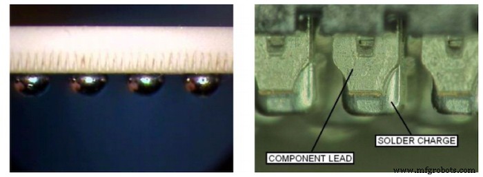
Figure 1. Solder balls on BGA vs. solder charges on Samtec’s SEAF8 / SEAM8
SEARAY’s 0.8 mm (SEAF8 / SEAM8 series) features alternating pitches of 0.80 mm and 1.20 mm, giving designers extra routing space between rows.
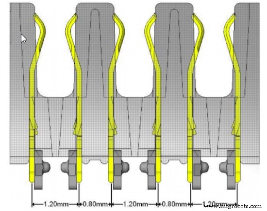
Figure 2. Alternating pitch of the SEAF8 / SEAM8
Keys to Achieving Better Solder Joints During Processing
Adhering to the manufacturer’s processing guidelines yields the highest success rate for soldering connectors. These guidelines often include PCB footprints, stencil layouts and thickness, solder screen‑printing specifications, placement tolerances, oven profiles, and rework procedures.
Footprint and Stencil
Samtec supplies more than 200,000 symbols and footprints for popular EDA tools—Altium, Circuit Studio, Eagle, Fusion 360, and others—allowing designers to download the exact footprint and stencil layout.
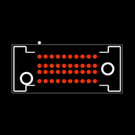
Figure 3. SEAF8 PCB footprint
Using the provided footprint and stencil increases the likelihood of achieving reliable solder joints.
Solder Screen Printing Process
Complete pad coverage is essential for a robust joint. The stencil aperture is deliberately larger than the pad to ensure that the solder charge contacts the paste, as shown in Figure 4.
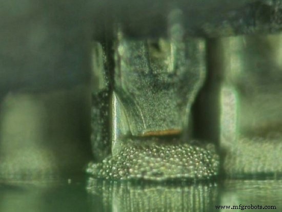
Figure 4. Solder charge location relative to the solder print with good contact between paste and solder charge.
If the paste does not fully cover the charge, wetting will fail. Automated inspection should reject any pad lacking full coverage, prompting cleanup and re‑printing.
Placing the Component
Automated pick‑and‑place machines ensure precise placement. The Z‑axis must seat the solder charges flush with the PCB surface. During reflow, the connector’s weight helps it settle, improving coplanarity, as illustrated in Figures 5 and 6.
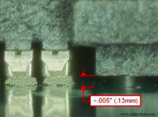
Figure 5. SEAF8 insulator housing fully seated prior to processing.
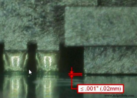
Figure 6. SEAF8 insulator housing fully seated after reflow.
Proper Oven Profiling
Lead‑free solder reflow profiles must comply with IPC/JEDEC J‑STD‑020: a peak temperature of 260 °C and 30 seconds above 255 °C. The following charts detail Samtec’s recommended temperature ranges.
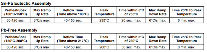
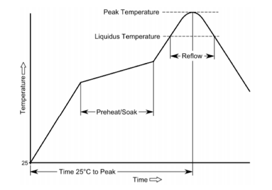
Figure 7. Samtec Recommended Temperature Profile Ranges (SMT)
A low‑oxygen environment—typically achieved by nitrogen infusion—enhances wettability. For high‑density connectors like SEAF8/SEAM8, processing should occur in a nitrogen‑rich atmosphere.
Accurate profiling of a fully populated board is critical. Monitoring the solder paste manufacturer’s temperature parameters ensures joints reach the desired temperature. Place a thermocouple through the board’s back, targeting the connector center, to verify the profile.
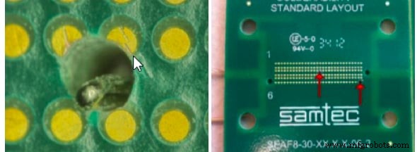
Figure 8. Thermocouple placement for oven profile.
Increasing Importance of Proper Processing
Even with advanced equipment, improper processing leads to reworks, scrap, and lost margins. As device sizes shrink and densities climb, the need for precise, repeatable processes grows. Samtec’s comprehensive footprints, stencil layouts, and processing guidance help designers achieve consistent, high‑quality assemblies.
Industry Articles are a form of content that allows industry partners to share useful news, messages, and technology with All About Circuits readers in a way editorial content is not well suited to. All Industry Articles are subject to strict editorial guidelines with the intention of offering readers useful news, technical expertise, or stories. The viewpoints and opinions expressed in Industry Articles are those of the partner and not necessarily those of All About Circuits or its writers.
Industrial equipment
- AI in Manufacturing: Three Key Trends Shaping 2019
- Solder Mask Discoloration on PCBs: Causes, Diagnostics, and Remedies
- Optimizing SMT Component Placement on PCBs for Reliability
- Robust PCBs for Extreme Conditions: Design, Benefits, and Applications
- Expert Guide: Troubleshooting Wave Soldering Issues on PCBs
- Mastering IPC Standards: A Comprehensive PCB Quality Guide
- Optimizing PCB Design for Manufacturing: Key Strategies & Best Practices
- Chevalier Vertical Turning Center: Integrated Hard Turning, Milling, Drilling, Tapping & Grinding for Large Parts
- PCB Technologies: The Next Frontier in Printed Circuit Boards
- The Critical Role of Integrated Cutting & Forming in Tube Processing