


BJT Transistors: The Cornerstone of Compact, Efficient Electronics Design
A study into the history of electronics will point out that transistors’ invention was crucial for humankind. Transistors are available to replace bulky, power-intensive, and low-efficiency vacuum tubes.
Currently, we use transistors either for amplification or switching in electronic circuits.
Check out this article to learn more about bipolar junction transistors, their configurations, and applications.
What is a BJT Transistor?
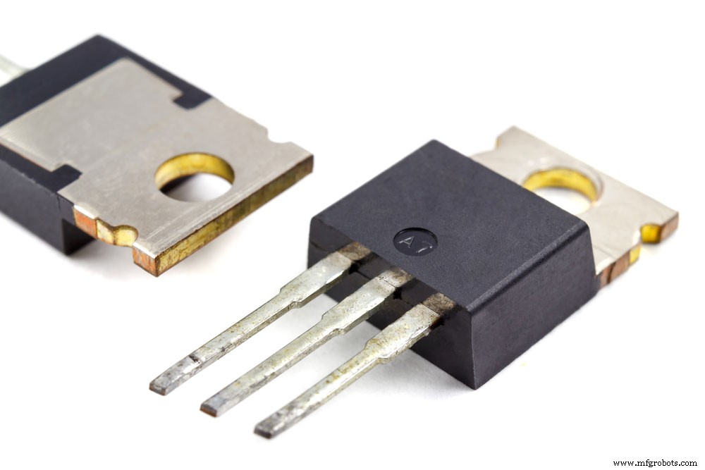
Fig 1: An NPN power transistor
A Bipolar Junction Transistor (BJT) is a current-controlled semiconductor device that comprises two n-p junctions.
It has three terminals; the base, the emitter, and the collector. Depending on the n-p arrangement, a BJT uses either the holes or the electrons as the primary charge carriers.
The application of a signal at the base terminal undergoes amplification at the collector terminal of the transistor. However, it requires some DC power for it to amplify the signal.
Configuration of BJT Transistors
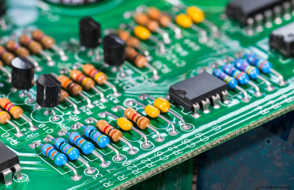
Fig 2: Electronic Components on a Circuit Board
A BJT is a three-terminal switching or amplifying device critical in electronic circuits. Depending on the primary charge carrier, it’s possible to develop two bipolar junction transistor configurations.
Therefore, in bipolar junction transistors, we’ve two inputs, but it’s impossible to have two outputs since it’s a three-terminal device.
One of the terminals is common for both input and output for overcoming an extra output terminal.
The following three are the possible BJT configurations.
BJT Transistors: The Common Emitter Configuration
Here, we apply the input signal between the base-emitter junction and the collector and emitter junction output. Therefore, the emitter inverts the input signal.
BJT Transistors: The common Collector Configuration
This configuration applies the input between the base-collector junction while taking the output from the collector-emitter corner.
The Common Base Configuration
Common Base configuration uses the base terminal for both input and output signals. The standard base configuration has only voltage gain but no current income.
BJT Characteristics
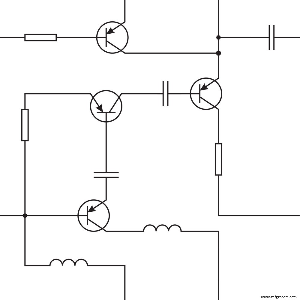
Fig 3: A Circuit Diagram With Transistors
The three BJT configurations result in different circuits with different characteristics. The most important features include input and output impedances, current, and voltage gains.
| Characteristics | Common Base | Common Emitter | Common Collector |
| Power Gain | Low | Very High | Medium |
| Current gain | Low | Medium | High |
| Voltage gain | High | Medium | Low |
| Phase angle | 0° | 180° | 0° |
| Output impedance | Very High | High | Low |
| Input Impedance | Low | Medium | High |
The standard emitter configuration is the most common BJT configuration. Therefore, its good power, voltage, and current gains improve circuit amplification.
Types of BJT Transistor

Fig 4: A Technician Checking an Electronic Circuit Board
Bipolar junction transistors are classified according to the leading charge carriers in their structure. As a result, we have
- PNP BJTs- Transistors with holes as the main charge carriers
- NPN BJTs- Transistors that use electrons as the main charge carriers.
NPN transistors are more popular than PNPs as they offer better amplification. NPN transistors have more electrons in their structure, and electrons have higher mobility than holes.
BJT Transistors: PNP Bipolar Junction Transistors
A PNP transistor is a bipolar junction transistor that involves doping an N-type material between two P-type semiconductor materials. The emitter supplies the positive charge carriers in PNP transistors, which pass through the base and onto the collector.
In this way, the base controls the number of charge carriers that pass from the emitter to the collector.
NPN Bipolar Junction Transistors
An NPN transistor is a bipolar junction transistor that involves doping a P-type semiconductor material between two N-type materials. In this case, the majority of charge carriers are free electrons.
The negative charge carriers move from the valence to the conduction bands when they’re sufficiently excited. Consequently, there will be some current flow through the N-type semiconductor region.
The Working Area of The BJT Transistor
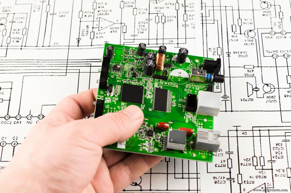
Fig 5: An Electronic Circuit Board
Transistors technically act as switches or amplification devices in electronic circuits. Bipolar junction transistors are three-terminal active devices that can either conduct or not depending on the gate bias.
Therefore, let’s look at the working areas of a BJT
Active Region
Here, the transistor works as an amplifier.
Ic = 𝞫.Ib
𝞫 is the ratio of the collector and base currents and provides the current gain for a common emitter transistor.
Saturation Region
The transistor is fully ON, with its base-collector and base-emitter junctions being in forwarding bias mode.
Ic = I(Saturation)
Cut-Off Region
Here, the transistor is entirely OFF, with its base voltage being less than both collector and emitter voltages.
Ic=0
BJT Transistors:Applications of BJTs
- Firstly, bipolar junction transistors function as demodulators or detectors
- Secondly, used in amplifier circuits as amplifiers or used as modulators
- Also, they operate oscillators and multivibrators
- Besides, they’re critical clipping circuits for waveshaping
- Furthermore, BJTs are also critical in time delay circuits
- Finally, BJTs operates in electronic switching circuits
Conclusion
Bipolar junction transistors are critical electronic components that require a deep understanding of a circuit. As a result, you might have seen them but not understood how they work.
We hope this article has cleared some mystery around BJTs and opened doors for you to proceed with your project.
For more information, clarification, or assistance on electronics, reach out to our experts.
Industrial Technology
- Bipolar Junction Transistors (BJT): Core Principles and Practical Applications
- Understanding Junction Field‑Effect Transistors (JFET): Fundamentals and Applications
- Understanding Insulated‑Gate Field‑Effect Transistors (IGFETs)
- Master E3.series for Industrial Equipment Design: Unified Electrical & Mechanical Engineering
- Professional Repairs and Support for Damaged Industrial Electronics
- Maximizing Machinery Longevity: Professional Heavy Equipment Repair & Maintenance Guide
- Master Electronic Enclosure Design: A Comprehensive Sheet Metal Guide
- Zero‑Crossing Detectors: Safeguarding Sensitive Electronics from Inrush Currents
- Key PCB Design Principles for Automotive Electronics
- Electronic Pumps Explained: Types, Uses, and Applications