


Understanding Junction Field‑Effect Transistors (JFET): Fundamentals and Applications
A transistor is a linear semiconductor device that controls current using a low‑power electrical signal. Transistors fall into two main families: bipolar and field‑effect. While bipolar transistors use a small current to regulate a large current, field‑effect transistors (FETs) rely on a small voltage for the same purpose. This article introduces the field‑effect concept and focuses on the junction field‑effect transistor (JFET).
All FETs are unipolar, meaning the primary current consists of either electrons in an N‑type semiconductor or holes in a P‑type semiconductor. This unipolar nature becomes evident in the device’s structure:
N‑channel JFET
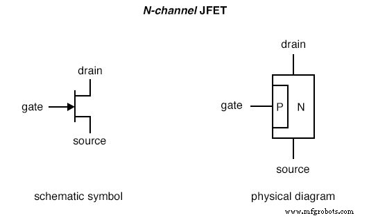
In a JFET, the controlled current flows between the source and drain terminals. The gate‑source voltage regulates this flow. Unlike bipolar devices, the current path does not cross a PN junction; instead, it traverses an uninterrupted semiconductor channel. The diagram above shows an N‑type channel; P‑type channels also exist.
P‑channel JFET
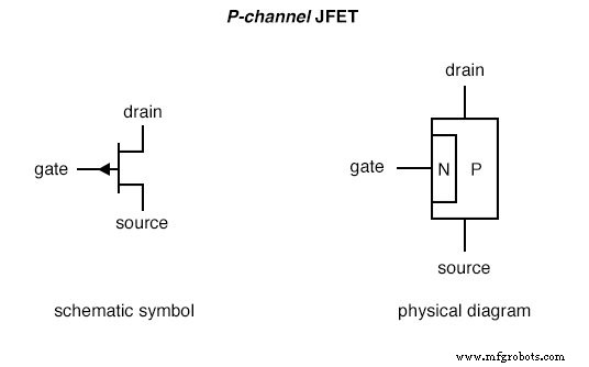
Although P‑channel JFETs are available, N‑channel devices are more commonly used due to semiconductor fabrication advantages. For practical purposes, the key difference between N‑ and P‑channel JFETs is the biasing of the gate‑channel PN junction.
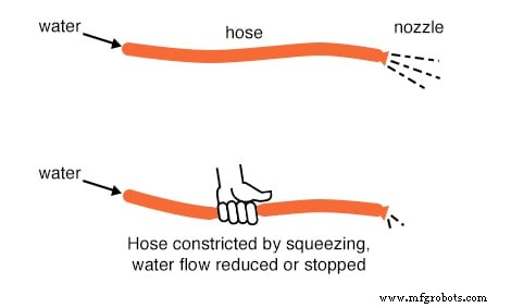
When no voltage is applied between gate and source, the channel offers a wide, unobstructed path for current. Applying a reverse‑bias voltage to the gate‑source PN junction reduces the channel’s conductivity. At a critical voltage, the depletion region expands to pinch off the entire channel, forcing the JFET into cutoff mode. This pinch‑off effect is analogous to squeezing a flexible hose until the flow stops.
JFETs are normally‑on devices: with no gate voltage, current flows freely. In contrast, bipolar transistors are normally‑off; without base current, collector‑emitter current is absent. The JFET’s current is controlled by a voltage signal, while bipolar transistors are controlled by a current signal. Moreover, the reverse‑biased gate‑source PN junction draws virtually no current, reinforcing the JFET’s classification as a voltage‑controlled device.
Forward‑biasing the gate‑source junction slightly increases the channel’s conductivity, but the junction is not designed to carry significant current, so forward bias should be avoided.
This overview provides the core principles of JFET operation. In the next section, we’ll examine the JFET’s role as a switching element.
RELATED WORKSHEETS:
- Junction field‑effect transistors (JFET) Worksheet
- JFET Amplifiers Worksheet
Industrial Technology
- JFET Current Regulator – Build and Test a Stable Constant‑Current Source
- Understanding Junction Field-Effect Transistors (JFETs): Gate Current Direction & N‑Channel vs P‑Channel
- Hybrid Transistor Design: IGFET‑BJT Combo for High Gain and Low Drop
- Understanding Bipolar Junction Transistors: Structure, Operation, and Amplification
- Junction Field‑Effect Transistors (JFET): Design, Operation, and Advanced Variants
- Insulated‑Gate Field‑Effect Transistors (MOSFETs) – Design, Operation, and Power Variants
- Bipolar Junction Transistors (BJT): Core Principles and Practical Applications
- Using a Junction Field‑Effect Transistor (JFET) as a Low‑Power On/Off Switch
- Understanding Insulated‑Gate Field‑Effect Transistors (IGFETs)
- Advanced Harmonics Management: Part 2 – Effective Strategies & Measurements