


Common-Emitter Amplifier Limitations: Distortion, Temperature, and High‑Frequency Challenges
In an ideal world a transistor would amplify signals with zero distortion, unlimited frequency reach, and handle large currents at high temperatures. In reality, every BJT exhibits non‑idealities that limit performance. This article explains the key quirks—nonlinearity, temperature drift, thermal runaway, junction capacitance, noise, and high‑frequency limits—and offers practical mitigation strategies.
Nonlinearity
The class‑A common‑emitter amplifier, driven close to clipping, shows a noticeably flatter positive peak than the negative peaks, as illustrated in the figure below. This distortion is unacceptable in high‑fidelity audio and many precision applications.
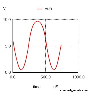
Large‑signal CE amplifiers are inherently nonlinear because transistor parameters such as β (current gain) vary with collector current. While β is high at low I₌, it decreases at very low or high currents, leading to harmonic distortion.
common-emitter amplifier
Vbias 4 0 0.74
Vsig 5 4 sin (0 125m 2000 0 0)
rbias 6 5 2k
q1 2 6 0 q2n2222
r 3 2 1000
v1 3 0 dc 10
.model q2n2222 npn (is=19f bf=150
+ vaf=100 ikf=0.18 ise=50p ne=2.5 br=7.5
+ var=6.4 ikr=12m isc=8.7p nc=1.2 rb=50
+ re=0.4 rc=0.3 cje=26p tf=0.5n
+ cjc=11p tr=7n xtb=1.5 kf=0.032f af=1)
.fourier 2000 v(2)
.tran 0.02m 0.74m
.end
spice -b ce.cir;
Fourier analysis v(2):
THD: 10.4688 %
The SPICE netlist above demonstrates how to quantify distortion. The ".fourier 2000 v(2)" command tells SPICE to analyze the output at 2000 Hz, yielding a total harmonic distortion (THD) of 10.47 % and a breakdown of individual harmonics. Reducing collector current or limiting the load line, and ultimately applying negative feedback, can markedly lower distortion.
Temperature Drift
Temperature influences both AC and DC transistor characteristics through environmental changes and self‑heating. Applications in military or automotive environments often require operation across a wide temperature range. Even in benign settings, high‑power circuits generate significant self‑heating.
Leakage current ICO and β increase with temperature. The DC β (hFE) grows exponentially, while the AC β (hfe) rises more slowly, typically doubling from –55 °C to 85 °C. This increase shifts the bias point, potentially clipping one side of the output waveform and amplifying bias drift in multi‑stage, direct‑coupled amplifiers. Negative feedback is the standard solution to stabilize both bias and AC gain.
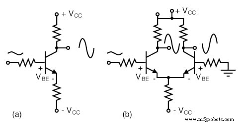
Figure (a) shows a single‑ended CE amplifier; as temperature rises, VBE drops below its nominal 0.7 V for silicon, increasing collector current and further shifting the bias point. Figure (b) presents a differential amplifier that cancels VBE drift when both transistors share the same temperature.
The maximum recommended junction temperature for silicon devices is 125 °C, though derating is advised for higher reliability. Beyond 150 °C, silicon transistor operation ceases. Silicon‑carbide or diamond transistors can tolerate substantially higher temperatures.
Thermal Runaway
Elevated temperature increases collector current, which in turn raises power dissipation and further raises temperature—a self‑reinforcing loop known as thermal runaway. The cure is a bias scheme that incorporates negative feedback to keep the bias point stable.
Junction Capacitance
Collector‑base (CCB) and emitter‑base (CEB) capacitances reduce high‑frequency gain. In a CE amplifier, CCB feeds back to the base, effectively multiplying its influence by β—the Miller effect. This reduces bandwidth significantly.
Noise
Transistor noise limits the sensitivity of small‑signal amplifiers. Shot noise from carrier flow in the base and thermal noise from device resistance are the primary contributors. Thermal noise rises with temperature.
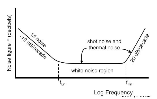
Noise figure (F) quantifies the excess noise added by the amplifier. It is expressed as a ratio of input to output signal‑to‑noise ratios, often reported in decibels (FdB). A good VHF transistor has F < 1 dB, while the figure climbs by about 20 dB per decade above VHF. Noise also increases at low frequencies (1/f noise) by ~10 dB per decade.
Figure below plots small‑signal transistor noise figure versus frequency, showing the trade‑offs for RF and low‑frequency designs.
Thermal Mismatch in Parallel Transistors
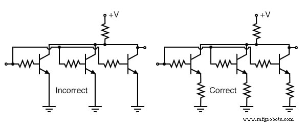
When identical power transistors are paralleled to increase current, mismatches in β and temperature cause unequal current sharing, potentially leading to thermal runaway. The solution is to add emitter ballast resistors (less than an ohm) to provide negative feedback, equalizing current flow. Mounting all transistors on a common heatsink also helps.
High‑Frequency Effects
As frequency rises, the common‑emitter small‑signal current gain (hfe) falls. The beta‑cutoff frequency fT marks the point where hfe = 1; practical amplifiers require f < 0.1 fT. Silicon bipolar devices are usable up to a few GHz; silicon‑germanium extends this to ~10 GHz.
Alpha‑cutoff frequency fα (where α = 0.707 · α0) is nearly equal to fT. The maximum oscillation frequency fmax is the highest frequency at which the transistor can sustain oscillations under optimal bias and matching; it is the absolute upper limit, though practical amplifiers never operate near fmax.
For example, the PN2222A has input capacitance Cobo = 9 pF and output capacitance Cibo = 25 pF. Due to the Miller effect, the effective base capacitance becomes β · CCB, magnifying the impact on bandwidth.
Choosing a high‑frequency transistor and employing a common‑base or cascode configuration can mitigate junction capacitance effects and extend bandwidth.
Review
- Distortion arises from β variation with collector current.
- Collector current, VBE, β, and junction capacitances vary with temperature.
- Temperature‑induced current increases can trigger thermal runaway.
- Junction capacitance, amplified by the Miller effect, limits high‑frequency gain.
- Noise figure measures excess noise and limits small‑signal amplification.
- Paralleling power transistors requires emitter ballast resistors to equalize current.
- fT is the absolute upper frequency limit for a CE amplifier; fmax is the theoretical maximum for oscillation.
Related Worksheets
- Class A BJT Amplifiers Worksheet
Industrial Technology
- Hands‑On Guide to Current Dividers: Build, Measure, and Simulate with a 6 V Battery
- Mastering SPICE: Common Quirks & How to Avoid Them
- Bipolar Junction Transistors (BJT): Core Principles and Practical Applications
- BJT Switching: How Transistors Efficiently Control High‑Current Loads
- Understanding BJT Active‑Mode Operation: From Cut‑Off to Saturation
- Decoding JFET Quirks: Common Pitfalls & How to Master Them
- Common IGFET Quirks & How to Mitigate Them
- Insulated‑Gate Bipolar Transistors (IGBTs): Merging FET Precision with BJT Power
- DIAC: The Bidirectional Trigger for AC Thyristors
- Understanding Electrical Resistance and Circuit Safety