


Understanding the NOT Gate (Inverter) in TTL Circuits
A single‑transistor inverter, while illustrative, lacks the performance required for real digital logic. Practical NOT gates employ multiple transistors to achieve high voltage gain, ensuring that the output transistor operates cleanly in either full cutoff or full saturation, and incorporate protective elements to guard against accidental damage.
Practical Inverter Schematic Diagram
Below is a complete schematic of a functional TTL NOT gate, incorporating all essential components for dependable, high‑gain operation:
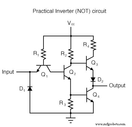
The design relies solely on resistors, diodes, and bipolar junction transistors (BJTs). Alternate topologies, such as those using field‑effect transistors (FETs), can also realize the NOT operation and are covered later in this guide.
NOT Gate Circuit Operation Analysis
High Input
First, consider the case where the input logic level is high (binary “1”). This scenario can be modeled by connecting the input pin to the supply voltage Vcc via a switch:
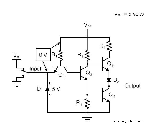
With the input driven high, diode D1 becomes reverse‑biased and conducts no current. Its sole purpose is to protect the transistor from accidental negative voltages applied to the input.
Under these conditions, the base‑emitter junction of transistor Q1 remains non‑conductive. However, Q1 is not used in the conventional sense; it functions as a pair of back‑to‑back diodes. The simplified schematic below illustrates this role:
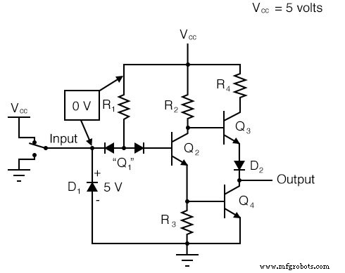
The two diodes in Q1 steer current to or away from the base of Q2, depending on the input logic level. To understand this steering action, imagine a simplified circuit consisting only of the base‑emitter junctions of Q2 and Q4 represented as single diodes, with the rest of the circuitry removed:
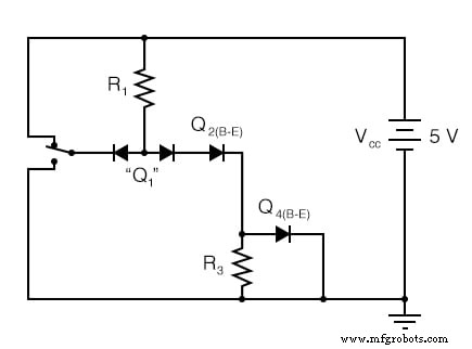
When the input switch is in the “up” position (connected to Vcc), no current flows through the left steering diode of Q1 because there is no voltage loop to drive electrons. However, current does flow through the right steering diode, the base‑emitter diode of Q2, and the base‑emitter diode of Q4:
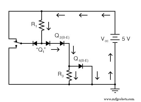
This means that in the actual inverter, Q2 and Q4 receive base current and turn on, allowing collector current to flow. The voltage dropped from the node at the junction of the two steering diodes to ground is approximately 2.1 V— the sum of three silicon PN junctions (the right steering diode, the base‑emitter junction of Q2, and the base‑emitter junction of Q4).
Low Input
Now, move the input switch to the “down” position and observe the resulting behavior:
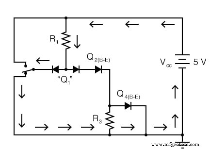
In this state, all the current flows through the left steering diode of Q1 and none through the right. Although a complete path appears to exist for current through the right diode and the series of Q4 and Q2, the forward voltage of the left diode (~0.7 V for silicon) is insufficient to forward‑bias the series string of the other two diodes, preventing any base current in Q2 or Q4. Consequently, both transistors remain in cutoff.
When the input is high, the left steering diode presents no voltage drop, allowing the right diode to conduct base current into Q2 via resistor R1:
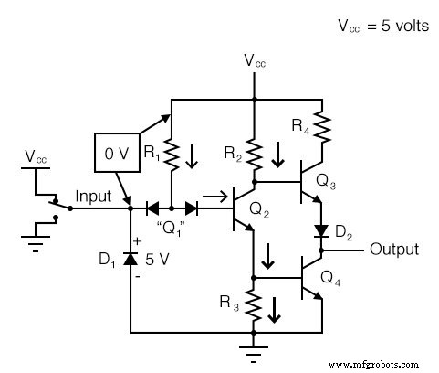
With sufficient base drive, Q2 saturates, pulling R3 low enough to forward‑bias the base‑emitter junction of Q4, which also saturates. The output node is then effectively shorted to ground, producing a logical “0”. The diode D2 prevents Q3 from turning on, keeping it in cutoff.
Low Input Output Analysis
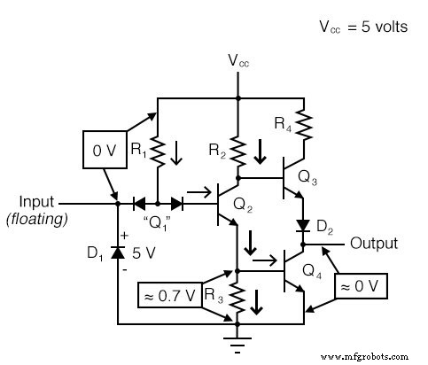
Conversely, when the input is low, current flows through the left steering diode of Q1, shutting Q2 and Q4 off. The base of Q3 receives sufficient voltage to forward‑bias its base‑emitter junction, driving it into saturation. The output rises to a high level (typically around 4 V, depending on load and saturation), satisfying the logical “1”. Thus, the inverter delivers a perfect logical inversion: a “1” input yields a “0” output and vice versa.
Circuit Observations
One noteworthy feature of this TTL inverter is that the input defaults to a high logic level when left floating. In that case, no current flows through the left steering diode, and the entire bias of R1 is applied to the base of Q2, turning it on and driving the output low:
Transistor‑to‑Transistor Logic (TTL)
The tendency of TTL gates to assume a high state when floating is a fundamental characteristic of the Transistor‑to‑Transistor Logic family. This behavior simplifies the design of gate outputs, especially when one gate’s output drives another’s input, because a TTL input only needs a path to ground to indicate a low state and can remain floating to indicate a high state.
Sourcing and Sinking Currents
Sourcing Currents
A TTL gate can both source and sink current through its totem‑pole output stage. When the output is high, the saturated Q3 connects the output node to Vcc, allowing current to flow from the load, through the emitter of Q3, and back up to the supply:
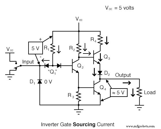
Conceptually, the output can be viewed as a double‑throw switch: when the gate outputs a high, the switch connects the output to Vcc; when it outputs a low, the switch connects the output to ground.
Sinking Currents
When the output is low, the Q4 transistor connects the output to ground, allowing current to flow from the supply, through the load, and into the emitter of Q4:
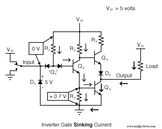
These dual capabilities—sourcing when high and sinking when low—are essential for driving a wide range of digital loads.
Requirements for TTL Operation
TTL inputs are designed to accept only a sinking current; they are inherently high when floating. Therefore, a gate driving a TTL input only needs to provide a sinking path to generate a low input. This eliminates the need for the driving gate to source current to the receiving input.
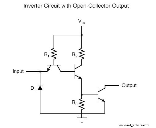
Open‑Collector Output
Because TTL inputs do not require current sourcing, the output stage can be simplified by removing Q3, resulting in an open‑collector configuration. The output can then be pulled high by an external resistor:
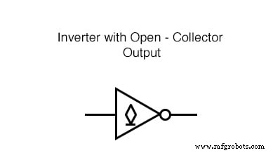
The standard symbol for an open‑collector inverter gate is shown below:
Review
- A NOT (inverter) gate produces the opposite logic level at its output: a low input yields a high output, and a high input yields a low output.
- TTL gates—constructed from resistors, diodes, and BJTs—offer high voltage gain and robust protection. Alternative families, such as FET‑based logic, are also available.
- When a gate “sources” current, it connects the output to the positive supply voltage, providing a high logic level.
- When a gate “sinks” current, it connects the output to ground, providing a low logic level.
- Totem‑pole outputs can both source and sink current, while open‑collector outputs can only sink. Open‑collector gates are well‑suited for driving TTL inputs because TTL inputs never need to source current.
Related Worksheets
- TTL Logic Gates Worksheet
- Basic Logic Gates Worksheet
Industrial Technology
- Understanding the Buffer Gate: Amplification and Signal Integrity in Digital Circuits
- Demystifying the XOR Gate: The Exclusive‑OR Function in Digital Logic
- BJT Switching: How Transistors Efficiently Control High‑Current Loads
- Understanding the Common-Emitter Amplifier: Switching, Amplification, and Biasing Techniques
- Understanding the Shockley Diode: A Comprehensive Guide to PNPN Thyristors
- DIAC: The Bidirectional Trigger for AC Thyristors
- Silicon‑Controlled Rectifiers (SCRs): Design, Operation, and Practical Applications
- Current Divider Circuits: Theory, Formula, and Practical Applications
- Chassis Wheels Shortage: How the Lack of Mobility is Stalling Global Supply Chains
- High-Current Voltage Regulator: The Complete Expert Guide