


Binary Signals and Logic Gates: Foundations of Digital Electronics
Although binary numeration is a fascinating mathematical construct, its true power emerges when applied to electronics. This chapter demonstrates how binary bits translate into real‑world circuit behavior.
The significance of binary numeration lies in its simplicity: a bit can only assume two values, 0 or 1. Any physical medium that can toggle between two saturated states can represent a bit. Thus, any system capable of storing binary bits can also encode and manipulate numerical values— the cornerstone of digital computing.
Binary and Electronic Circuits
Transistor Binary Operation
Transistors, when biased at their limits, operate in one of two discrete states: cut‑off (no controlled current) or saturation (maximum controlled current). A circuit designed to force a transistor into either extreme—avoiding the linear or active region—serves as a physical embodiment of a binary bit.
Voltage Levels as Bit Values
A transistor‑based circuit can output a voltage that represents a single bit: a low voltage denotes a binary “0”, while a relatively high voltage represents a binary “1”. Consider the following configuration:
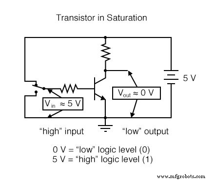
In this setup, the transistor is saturated by a 5‑V input applied through a two‑position switch. The saturated transistor drops negligible voltage across collector‑to‑emitter, yielding an output of virtually 0 V. Interpreting this, the input is a binary “1” and the output is a binary “0”. Any voltage close to the supply rail (relative to ground) is treated as “1”, whereas the absence of voltage is treated as “0”. These levels are commonly referred to as high (for “1”) and low (for “0”). The collective representation of a bit via a circuit voltage is called a logic level.
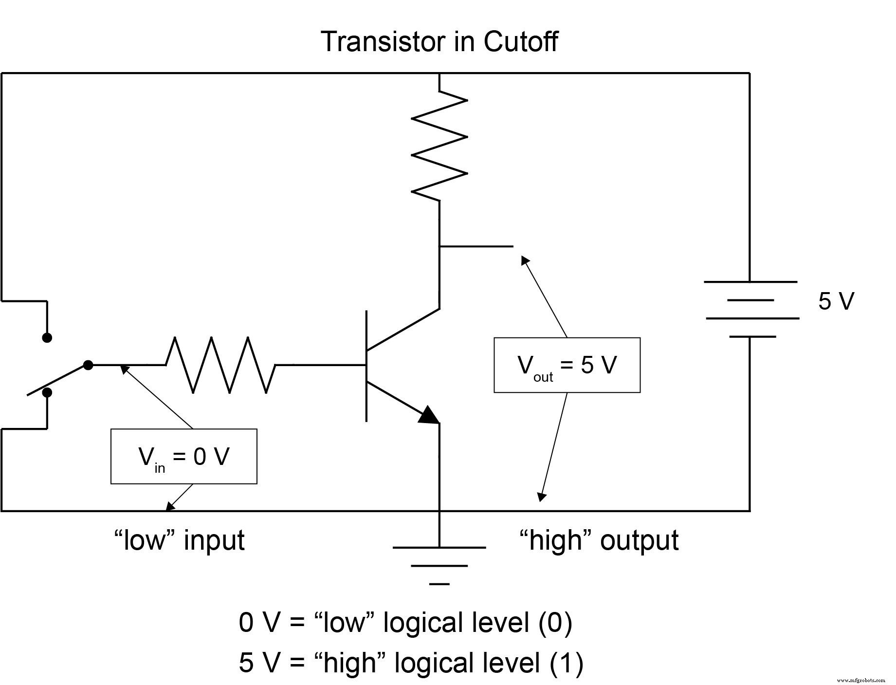
Reversing the Switch
Moving the switch to its alternate position applies a binary “0” at the input, producing a binary “1” at the output:
What Are Logic Gates?
By employing a single transistor, we create a basic logic gate, a specialized amplifier that accepts and generates logic‑level voltages corresponding to binary 1’s and 0’s. Gates are not meant for amplifying analog signals; instead, multiple gates combine to store bits (memory) or perform calculations (computation). The subsequent chapters will explore these uses in depth; for now, focus on individual gate behavior.
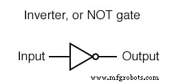
Inverter or NOT Gate
The circuit above functions as an inverter (or NOT gate) because it outputs the logical complement of its input. For clarity, gate circuits are typically depicted by dedicated symbols rather than by their transistor and resistor constituents. The standard symbol for an inverter is shown below:
An alternative representation is also common:

Notice the triangular shape, reminiscent of an operational amplifier. The small bubble at the input or output terminal indicates inversion. Removing the bubble yields a buffer symbol, which denotes non‑inverting amplification.
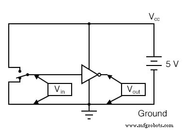
In digital schematics, power supply connections are often omitted for brevity. However, a complete representation of the NOT gate includes the supply rails, as illustrated below:
To streamline schematics, the power lines are frequently excluded, leaving only the essential input and output connections:
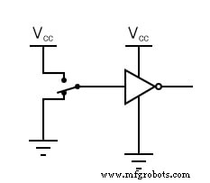
Here, Vcc denotes the positive DC supply voltage—typically 5 V—connected to the transistor’s collector. All points labeled Vcc share this connection.
Future sections will introduce additional logic gates with multiple inputs. The output of each gate depends on its input states and its logical function.
Expressing Gate Functions with Truth Tables
Truth tables are the standard tool for illustrating a gate’s behavior. They list every possible combination of input logic levels (high/low or 1/0) alongside the resulting output. For the single‑input NOT gate, the truth table is straightforward:
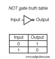
More complex gates have larger tables. A gate’s number of rows equals 2 raised to the power of its input count: 2 rows for one input, 4 rows for two inputs, 8 rows for three inputs, and so forth.
REVIEW:
- In digital circuits, binary bits (0 and 1) are represented by voltage levels relative to ground: no voltage equals “0”, and full supply voltage equals “1”.
- A logic gate is a specialized amplifier that inputs and outputs logic‑level voltages. Schematics usually use a unique symbol rather than a transistor‑resistor network.
- Power supply lines are commonly omitted in schematics for simplicity, mirroring the practice with operational amplifiers.
- Truth tables systematically capture the input–output relationship of a gate, enumerating all possible logic level combinations.
RELATED WORKSHEETS:
- Digital Logic Signals Worksheet
- Basic Logic Gates Worksheet
- Boolean Algebra Worksheet
Industrial Technology
- Mastering Voltmeter Use: Accurate Voltage Measurement Made Simple
- Essential DC Circuit Equations and Laws for Engineers
- Octal and Hexadecimal Numeration: A Practical Guide for Engineers
- Passive Averager and Op‑Amp Summer Circuits: From Averaging to Addition
- Understanding Voltage and Current: The Foundations of Electrical Flow
- Analog and Digital Signals: Foundations of Industrial Instrumentation
- Capacitors & Calculus: How Voltage Change Drives Current
- Precise Power Measurement Using Digital and Analog Multimeters
- Accurate Voltage Measurement with Digital and Analog Multimeters – A Step-by-Step Guide
- Digital PCBs: The Backbone of Modern Electronic Systems