


Understanding the Shockley Diode: A Comprehensive Guide to PNPN Thyristors
Our journey into thyristors starts with the four‑layer PNPN device, commonly called a Shockley diode after its inventor, William Shockley. It should not be confused with the Schottky diode, which is a two‑layer metal‑semiconductor junction known for its rapid switching.
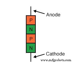
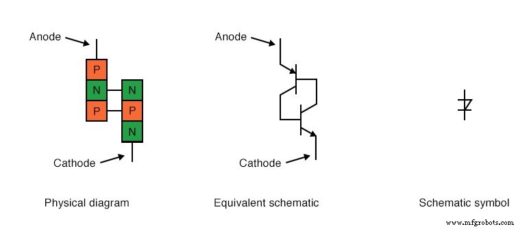
Textbooks often depict the Shockley diode as a simple four‑layer stack of P‑N‑P‑N material (see Figure 1). While the illustration is easy to understand, it does little to explain how the device actually functions.
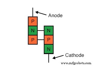
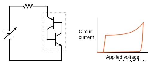
To illuminate its internal structure, a more detailed rendering (Figure 2) shows the device as two interconnected bipolar transistors—one PNP and one NPN—sharing common emitter and collector regions. When drawn with standard schematic symbols and proper doping concentrations, the Shockley diode appears as illustrated in Figure 3.
Connecting the Device to a Variable Voltage Source
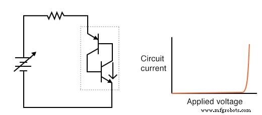
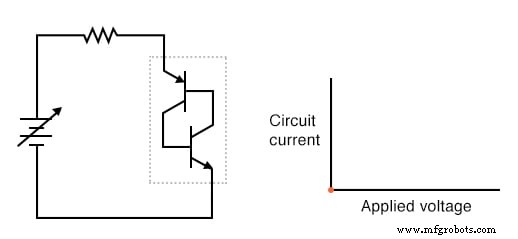
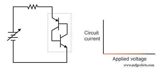
When no voltage is applied, no current flows. As the voltage is increased, the device remains non‑conductive because both transistors stay in cutoff. This happens because each transistor’s base current is controlled by the other; neither can turn on without the other being on—an “idealized catch‑22.”
How a Shockley Diode Turns On and Off
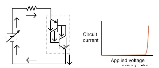
Real transistors differ from the ideal model: they can withstand a finite collector‑emitter voltage before breakdown occurs. In the Shockley configuration, once the applied anode‑to‑cathode voltage exceeds the breakover threshold of one transistor, it starts conducting. This conduction supplies base current to the other transistor, turning it on in the usual way. The result is a mutually reinforcing loop: both transistors saturate, keeping the device latched in the on state.
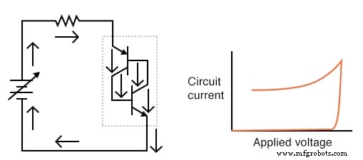
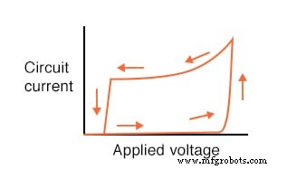
To return the device to the off state, the applied voltage must be reduced below the low‑current dropout level. At that point, one transistor falls into cutoff, eliminating base current to the other, and the entire structure reverts to the off state.
Voltage–Current Characteristics and Hysteresis
The I‑V relationship of a Shockley diode exhibits classic hysteresis. With zero applied voltage, the current is zero (Figure 4). As voltage rises, the current stays near zero until the breakover point is reached (Figure 5). At this moment, one transistor breaks down, triggering the other and producing a sharp rise in current (Figure 6). Even when the voltage is subsequently reduced, the device remains on until the current falls below the dropout threshold (Figure 7). If the voltage is reduced further, the current drops sharply, and the device turns off (Figure 8). The resulting curve shows a distinct loop, confirming the device’s binary on/off nature (Figure 9).
Key Terminology
- Latched – the device remains on once triggered.
- Firing – the act of initiating the latched state, usually by exceeding the breakover voltage.
- Breakover – the voltage at which one transistor begins to conduct in breakdown, leading to latch‑up.
- Dropout – the low‑current threshold below which the device returns to the off state.
- Critical Rate of Voltage Rise – the maximum dv/dt that the diode can withstand without unintended latching.
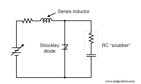
Diodes can also fire due to rapid voltage changes (dv/dt). The intrinsic junction capacitances act as temporary current sources that can trigger the transistors if the voltage rises too quickly. To mitigate this, designers employ series inductors and parallel RC snubber networks (Figure 10) to limit dv/dt and protect the device.
Quick Review
- Shockley diodes are PNPN four‑layer devices that function as a pair of coupled PNP and NPN transistors.
- Like all thyristors, they latch on once fired and stay on until the current falls below dropout.
- Firing occurs by exceeding either the breakover voltage or the critical dv/dt.
- Unlatched state is achieved by reducing current below the dropout threshold.
Industrial Technology
- Using a Transistor as an Electrically Controlled Switch
- Sensitive Static‑Electricity Detector Using a JFET Switch
- Understanding the NOT Gate (Inverter) in TTL Circuits
- BJT Switching: How Transistors Efficiently Control High‑Current Loads
- Understanding the Common-Emitter Amplifier: Switching, Amplification, and Biasing Techniques
- Precision Transistor Biasing: Calculating Resistors for Stable Amplifier Performance
- Insulated‑Gate Bipolar Transistors (IGBTs): Merging FET Precision with BJT Power
- DIAC: The Bidirectional Trigger for AC Thyristors
- Unijunction Transistor (UJT) & Programmable UJT (PUT): Design, Operation, and Oscillator Applications
- Silicon‑Controlled Switch (SCS): Design, Operation, and Forced Commutation