


Unijunction Transistor (UJT) & Programmable UJT (PUT): Design, Operation, and Oscillator Applications
What is a Unijunction Transistor (UJT)?
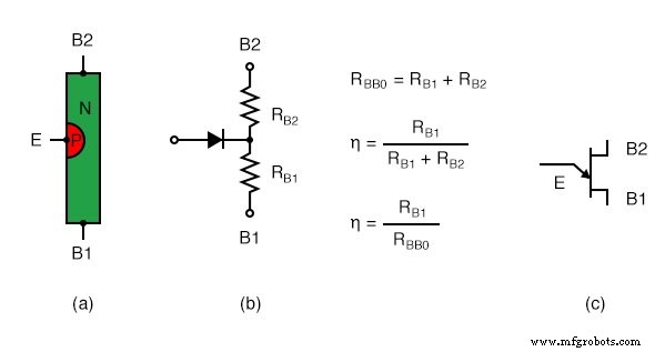
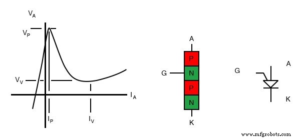
A UJT is a three‑terminal silicon device that, although not a thyristor, can trigger larger thyristors by delivering a sharp pulse to its base‑B1. It is built from an N‑type silicon bar with a centrally located P‑type region. The two ends of the bar are the bases B1 and B2; the central P‑type region acts as the emitter. When the emitter is disconnected, the total base‑to‑base resistance (R_BBO) equals the sum of R_B1 and R_B2 and typically ranges from 4 kΩ to 12 kΩ, depending on the device. The intrinsic standoff ratio (η)—the ratio of R_B1 to R_BBO—varies from 0.4 to 0.8. The schematic symbol is shown in Figure (c).
Electrical Characteristics
The emitter‑current versus emitter‑voltage curve (Figure (a)) demonstrates that as the emitter voltage (V_E) increases, the emitter current (I_E) rises to a peak value (I_P). Beyond this point, the device enters a negative‑resistance region where the current decreases as voltage falls, reaching a minimum at the valley point (V_V). The resistance of R_B1 is lowest at this valley. For a 2N2647, the datasheet lists I_P = 2 µA and I_V = 4 mA.
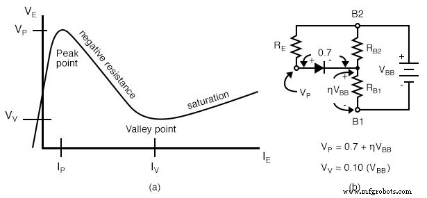
The peak voltage (V_P) equals the voltage drop across R_B1 plus a ~0.7 V diode drop. The valley voltage (V_V) is typically about 10% of the base‑to‑base supply (V_BB).
Relaxation Oscillator Using a UJT
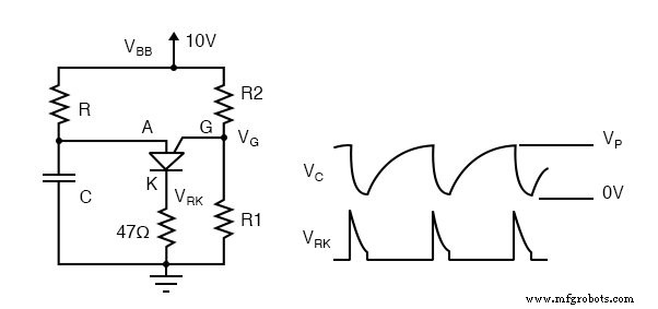
In a UJT‑based relaxation oscillator, a charging resistor (R_E) charges a capacitor (C_E) until the emitter voltage reaches V_P. At this instant the low resistance between emitter and B1 discharges the capacitor rapidly. When the capacitor voltage falls below V_V, the emitter‑B1 resistance rises again, allowing the capacitor to recharge and the cycle repeats. The approximate period is T ≈ R_E·C_E, but a more accurate expression is given in the figure.
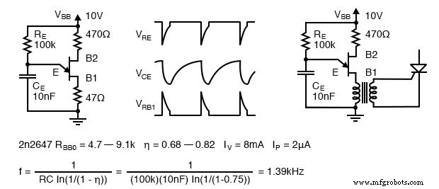
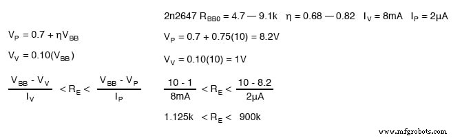
The discharge pulse can appear across the external B1 and B2 load resistors. The resistor at B1 should be low enough not to affect the discharge time; the B2 resistor is optional and may be shorted. The charging resistor must be chosen such that it can supply I_P at V_BB - V_P and limit the valley current to I_V at V_BB - V_V. For a 2N2647, the calculations are shown in the figure.
Programmable Unijunction Transistor (PUT)
The PUT is a three‑terminal, four‑layer thyristor that behaves like a UJT but is available in mass production and at low cost. Its gate—an N‑type layer near the anode—is called an “anode gate” and is connected to the anode in the schematic symbol. The PUT’s characteristic curve (anode current vs. anode voltage) mirrors that of a UJT; the gate voltage sets the programmable peak voltage (V_P). External resistors (R1 and R2) replace the internal R_B1 and R_B2, allowing designers to program the intrinsic standoff ratio (η = R1/(R1+R2)).
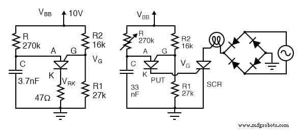
In a PUT relaxation oscillator, a resistor (R) charges a capacitor until V_P is reached. The device then conducts heavily, pulling the operating point down the negative‑resistance slope to the valley, and a current spike flows through the cathode. After discharge, the point resets to the upward slope. The resistor must be large enough that it never supplies the valley current (I_P), but small enough to reach V_P during charging. For a 2N6027 with a 10 V supply and η ≈ 2/3, the acceptable resistor range is 143 kΩ < R < 755 kΩ.
Example Parameter Table for 2N6027 PUT
| Parameter | Conditions | Min | Typical | Max | Units |
|---|---|---|---|---|---|
| V_T | V_S=10 V, R_G=1 MΩ | 0.2 | 0.7 | 1.6 | V |
| V_T | V_S=10 V, R_G=10 kΩ | 0.2 | 0.35 | 0.6 | V |
| I_P | V_S=10 V, R_G=1 MΩ | - | 1.25 | 2.0 | µA |
| I_P | V_S=10 V, R_G=10 kΩ | - | 4.0 | 5.0 | µA |
| I_V | V_S=10 V, R_G=1 MΩ | - | 18 | 50 | µA |
| I_V | V_S=10 V, R_G=10 kΩ | 70 | 150 | - | µA |
| I_V | V_S=10 V, R_G=200 Ω | 1500 | - | - | µA |
| V_F (I_F=50 mA) | - | - | 0.8 | 1.5 | V |
With these values, a practical PUT relaxation oscillator can drive an SCR lamp dimmer. The circuit uses a V_BB unfiltered supply, a bridge rectifier, and a variable resistor that must be paired with a minimum series resistor to prevent the pot from being stuck at the valley point after each zero crossing.
Performance Considerations
- PUT timing circuits are typically usable up to 10 kHz.
- If a linear voltage ramp is required instead of an exponential one, replace the charging resistor with a constant‑current source (e.g., a FET‑based constant‑current diode).
- A DIY PUT can be constructed from a PNP and NPN transistor by omitting the cathode gate and using the anode gate.
Key Takeaways
- A UJT comprises two bases and a central emitter; its emitter‑B1 junction exhibits negative resistance.
- A PUT is a three‑terminal thyristor that emulates a UJT, with an external resistor network setting the intrinsic standoff ratio.
- Both devices are ideal for relaxation oscillators, timing circuits, and thyristor triggering.
Related Resources
- Thyristors Worksheet
Industrial Technology
- The 555 Integrated Circuit: A Timeless Benchmark in Analog Design
- The Quadratic Formula: A Reliable Tool for Solving Second‑Degree Equations
- BJT Switching: How Transistors Efficiently Control High‑Current Loads
- Using a Junction Field‑Effect Transistor (JFET) as a Low‑Power On/Off Switch
- Understanding the Shockley Diode: A Comprehensive Guide to PNPN Thyristors
- Silicon‑Controlled Switch (SCS): Design, Operation, and Forced Commutation
- Transistor vs. Resistor: Key Differences Explained
- Choosing the Right Transistor Replacement: A Guide to Optimal Selection
- Thyristor vs. Transistor: Core Differences Explained for Power Electronics
- TIP31C Transistor Pinout & Technical Guide for NPN Power Applications