


Using a Junction Field‑Effect Transistor (JFET) as a Low‑Power On/Off Switch
Field‑effect transistors are common in power‑switching applications. This article explains how a junction field‑effect transistor (JFET) can serve as an efficient on/off switch in a simple lamp circuit.
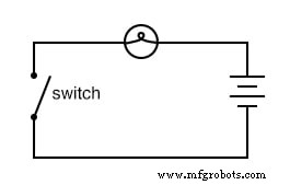
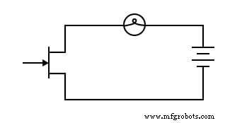
The JFET’s conduction path runs between its source and drain terminals. In the schematic below, the JFET’s source and drain are connected to the two ends of the lamp, exactly as a mechanical switch would be wired.
Unlike a bipolar junction transistor, a JFET’s source and drain are electrically indistinguishable on the symbol. In practice, most JFETs conduct reliably in either direction, so the two terminals can be interchanged without affecting performance.
JFET as an Opened Switch
With no voltage applied between gate and source, the JFET’s channel is fully open and the lamp receives full current. To turn the lamp off, a reverse‑biased DC voltage is applied between gate and source:
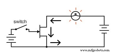
JFET as a Closed Switch
Applying a sufficient reverse bias expands the gate‑source depletion region, “pinching off” the channel and forcing the JFET into cutoff. This action turns the lamp off.
The gate draws virtually no current because it is a reverse‑biased PN junction. As a voltage‑controlled device, the JFET requires negligible input power, which is a key advantage over bipolar transistors.
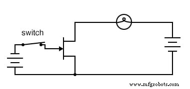
However, once the reverse bias is removed, the JFET may remain off. The gate‑source junction has a small capacitance that can retain the reverse‑bias voltage as stored charge. To allow the transistor to return to the on state, a bleed resistor is placed between gate and source:
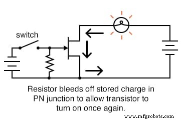
The resistor’s value is not critical; even a high‑value resistor provides a fast RC discharge that clears the stored charge quickly.
Any voltage source that can supply a few volts DC is sufficient to control the JFET. The required voltage, known as the pinch‑off or cutoff voltage, varies with each JFET’s design and is not a universal constant.
Key Points
- JFETs control source‑drain current via a voltage applied between gate and source.
- They are normally on; a reverse‑biased gate expands the depletion region, pinching off the channel.
- A bleed resistor may be needed to discharge the gate‑source capacitance and restore the on state after the control voltage is removed.
Related Worksheets
- Junction field‑effect transistors (JFET) Worksheet
Industrial Technology
- Using a Transistor as an Electrically Controlled Switch
- Understanding Junction Field-Effect Transistors (JFETs): Gate Current Direction & N‑Channel vs P‑Channel
- Understanding the PN Junction: From Structure to Diode Behavior
- Junction Field‑Effect Transistors (JFET): Design, Operation, and Advanced Variants
- BJT Switching: How Transistors Efficiently Control High‑Current Loads
- Understanding Junction Field‑Effect Transistors (JFET): Fundamentals and Applications
- Accurate Multimeter Testing of JFET Continuity and Pin‑Off Behavior
- JFET Transistor Ratings & Package Overview – Choosing the Right Device
- Unijunction Transistor (UJT) & Programmable UJT (PUT): Design, Operation, and Oscillator Applications
- Silicon‑Controlled Switch (SCS): Design, Operation, and Forced Commutation