


Understanding the PN Junction: From Structure to Diode Behavior
The PN junction is the cornerstone of modern semiconductor devices, turning a single crystal into a self‑sustaining voltage barrier that governs diode behavior. By doping one side of a crystal with acceptor atoms (P‑type) and the other with donor atoms (N‑type), a region of immobile charge forms at their interface. This depletion region acts as an intrinsic insulator, yet it is the very feature that allows the PN junction to function as a one‑way valve for electrical current.
Structure of a PN Junction
When a P‑type block is placed next to an N‑type block, the two materials simply touch and share no unique electrical properties—each remains a conductor with no net charge. The difference emerges when a single crystal is doped with P‑type material on one end and N‑type material on the other. The majority carriers are holes in the P side and electrons in the N side, and they are free to move through the lattice.
Formation of the Depletion Region
Near the junction, electrons diffuse from the N side into the P side, where they recombine with holes. The N side loses electrons and becomes positively charged; the P side gains electrons and becomes slightly negative. This creates a thin, immobile layer—called the depletion region—that is free of majority carriers and behaves like an insulator.
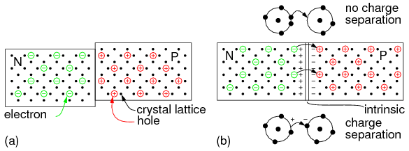
(a) Separate blocks of P and N semiconductor show no exploitable properties. (b) A single crystal doped with P and N material forms a potential barrier.
Potential Barrier and Biasing
The charge separation at the junction creates a built‑in potential barrier. The magnitude of this barrier depends on the semiconductor material: ~0.6–0.7 V for silicon, lower for germanium. An external voltage must exceed this barrier to allow current flow.
Forward Bias
Connecting the battery so that its negative terminal feeds electrons to the N side and its positive terminal removes electrons from the P side pushes majority carriers toward the junction. Once the applied voltage surpasses the barrier (≈0.6 V in silicon), electrons and holes recombine, and the depletion region shrinks, allowing current to flow.
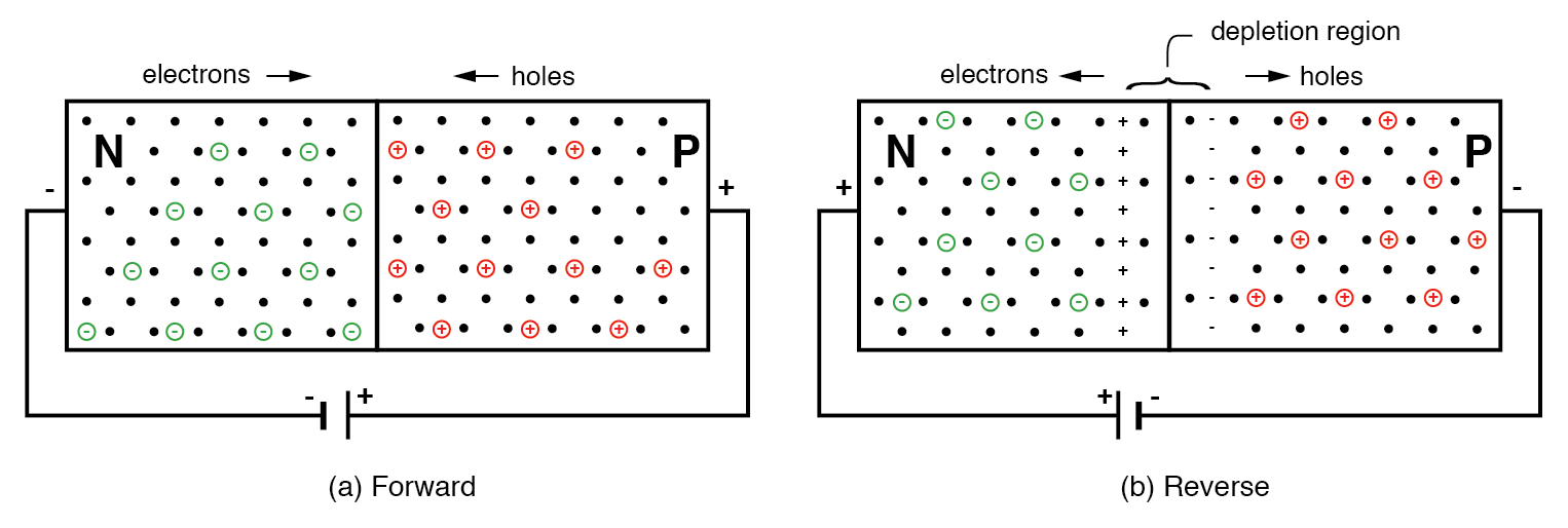
(a) Forward bias drives carriers into the junction, enabling recombination and current flow. (b) Reverse bias pulls carriers away, widening the depletion region and blocking current.
Reverse Bias
Reversing the battery polarity pulls majority carriers away from the junction, increasing the depletion width. No significant current flows except for a tiny leakage current, and the device is protected from destructive breakdown by selecting a reverse voltage rating above any operating voltage.
Diode Characteristics
The diode symbol reflects this behavior: the arrow (anode) points toward the P side, and the bar (cathode) points toward the N side. Forward bias current rises steeply once the barrier is overcome. In silicon diodes, the forward voltage (VF) is 0.6–0.7 V; in germanium it is ~0.2 V; in LEDs it can reach several volts.
The forward current range varies widely—from milliamps for small signal diodes to thousands of amperes for power diodes. Reverse leakage currents are typically <1 µA for silicon small‑signal devices, increasing with temperature. Breakdown occurs at high reverse voltages (50–800 V for silicon), necessitating a series resistor to protect the device.
Leakage is partly intrinsic—thermal generation of electron‑hole pairs—and partly due to surface conduction caused by contamination. Germanium diodes exhibit much higher leakage and are rarely used today.
Key Takeaways
- PN junctions are created by doping a monocrystalline semiconductor with both P‑type and N‑type regions.
- Electron diffusion across the junction creates a voltage barrier of ~0.6–0.7 V in silicon.
- Forward bias overcomes this barrier, enabling current flow through recombination at the junction.
- Reverse bias widens the depletion region, limiting current to a small leakage that rises with temperature.
- Leakage currents are <1 µA in small silicon diodes and are temperature dependent.
Further Reading
Industrial Technology
- BJT Switching: How Transistors Efficiently Control High‑Current Loads
- Using a Junction Field‑Effect Transistor (JFET) as a Low‑Power On/Off Switch
- Localizing Battery Supply Chains: Enhancing Security, Sustainability, and Cost Efficiency
- Self‑Powered Sensors: Eliminating the Battery Barrier for Ubiquitous IoT
- Calculate Battery Charging Time & Current: Step‑by‑Step Guide with 120Ah Example
- Consequences of Connecting a Battery to an AC Power Source
- Impact of Reverse Polarity Wiring on Battery Health
- Calculate the Ideal Battery Bank Size: A Practical Guide & Calculator
- DIY Battery Chargers: The Ultimate Guide to Building and Choosing the Best Designs
- Meeting the Rising Demand for Batteries: Strategies & Solutions