


Understanding Electrons, Holes, and Doping in Semiconductors
Pure semiconductors exhibit much higher resistivity than metals, yet they are far less insulating than materials such as glass. For an intrinsic (undoped) semiconductor to function effectively, its purity must reach at least one defect per 10 billion atoms—an equivalent to a single grain of salt in a railroad boxcar of sugar. Introducing intentional impurities—doping—significantly boosts conductivity, though it still falls short of metallic levels. Understanding why requires examining the material’s electron structure (see Figure).
Electron Structure
Figure (a) shows four valence electrons in a semiconductor atom forming covalent bonds with four neighboring atoms. All electrons are locked in these bonds, leaving no free charge carriers; consequently, an intrinsic semiconductor behaves as a relatively good insulator compared with metals.
(a) An intrinsic semiconductor is an insulator with a filled valence shell. (b) Thermal excitation can liberate a few electron‑hole pairs, giving rise to weak conduction.
Thermal energy occasionally frees an electron from the crystal lattice, as illustrated in Figure (b). The liberated electron can move freely through the lattice, while the vacancy it leaves behind carries a positive charge—a hole. Both electrons and holes contribute to current flow; the electron eventually recombines with a hole when it falls back into the lattice. When an external electric field is applied, electrons and holes drift in opposite directions. Increasing temperature creates more carriers, thereby reducing resistance—a behavior opposite to that of metals, where resistance rises with temperature due to increased scattering. In an intrinsic semiconductor the numbers of electrons and holes are equal, but their mobilities differ.
Semiconductor Impurities
Pure semiconductors alone are rarely useful; they must first be refined to a very high degree of purity. A material that is 1 part in 10 billion pure can then be doped with impurities at roughly 1 part in 10 million to raise the carrier density. This intentional addition of foreign atoms—called doping—transforms the crystal into a conductor that rivals metals.
Adding an electron donor (N‑type dopant) such as phosphorus increases the number of negative charge carriers. Donors belong to group VA (nitrogen, phosphorus, arsenic, antimony). Phosphorus, for example, has five valence electrons; it bonds with four silicon atoms and retains one loosely bound electron that becomes free to move. With a doping concentration of 1 ppm (1 part in 10 million), the resulting electron density far exceeds that of intrinsic silicon, enabling strong conduction in the conduction band.
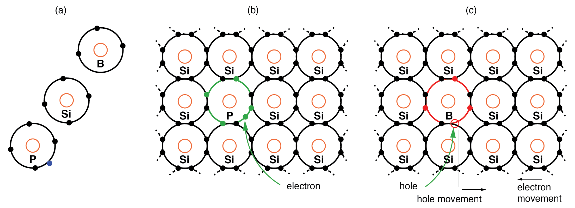
(a) Outer‑shell configurations of donor N‑type phosphorus, silicon, and acceptor P‑type boron. (b) N‑type donor impurity creates a free electron. (c) P‑type acceptor impurity creates a hole, a positive charge carrier.
Conversely, introducing an electron acceptor (P‑type dopant) with only three valence electrons—such as boron—creates a vacancy, or hole, in the lattice. Boron attempts to form four covalent bonds but can only supply three electrons, leaving an empty site that acts as a mobile positive carrier in the valence band. P‑type elements come from group IIIA (boron, aluminum, gallium, indium); boron is the standard dopant for silicon and diamond, while indium is used for germanium.
The “marble‑in‑a‑tube” analogy illustrates how holes move: an electron moving left to right vacates a spot that appears to move rightward. Electrons in an N‑type material drift to the right under an electric field, whereas holes in a P‑type material drift to the right, corresponding to electrons moving left.
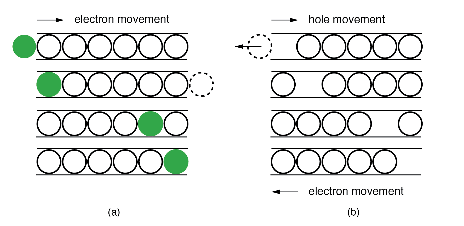
Marble‑in‑a‑tube analogy: (a) Electrons flow right in the conduction band. (b) Holes flow right in the valence band.
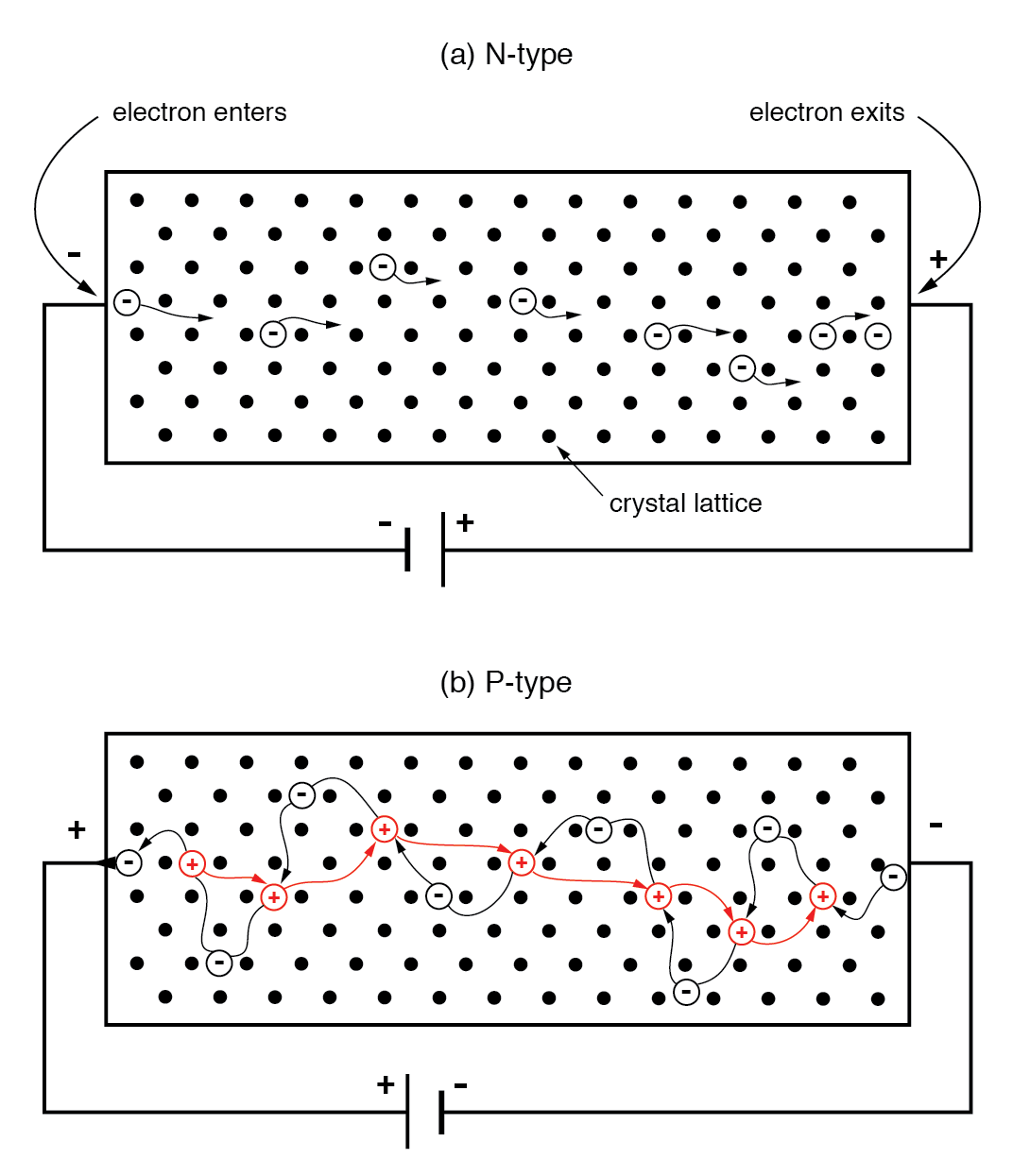
In an N‑type semiconductor, majority carriers are free electrons. When a voltage is applied, electrons enter the negative side, traverse the lattice, and exit the positive side, forming a current analogous to a metallic wire.
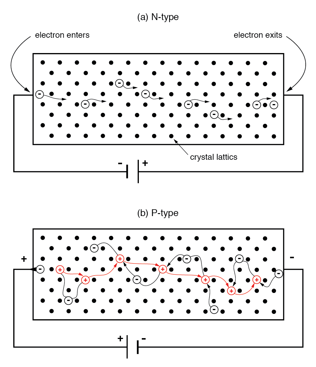
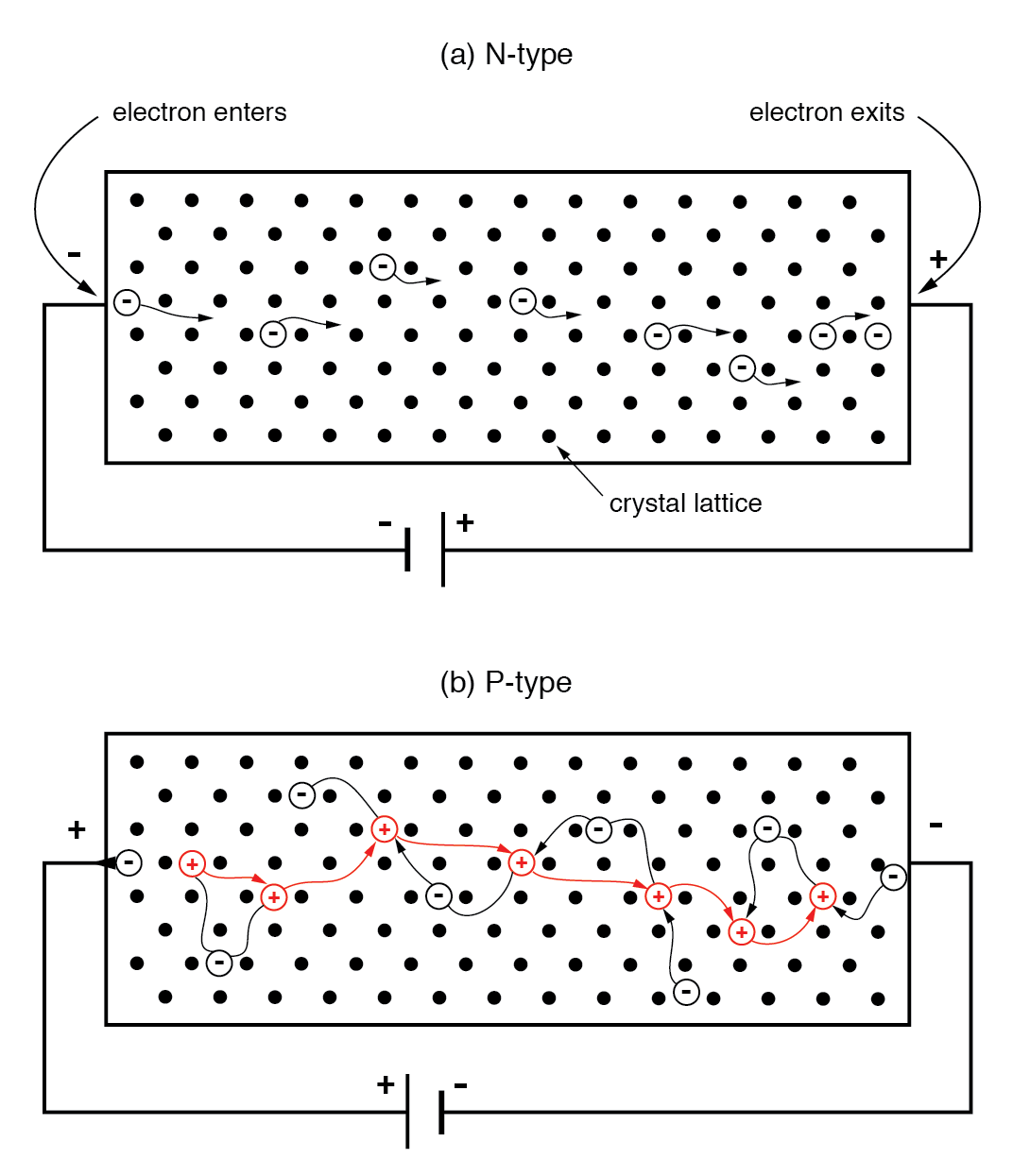
(a) N‑type semiconductor: electrons move left to right. (b) P‑type semiconductor: holes move left to right, equivalent to electrons moving right to left.
In a P‑type bar, holes are the majority carriers. A reversed battery polarity causes electrons to leave the left end for the positive terminal, creating a hole that moves rightward. At the negative end, a battery electron recombines with a hole, allowing another hole to enter from the left. The apparent hole motion is thus driven by electrons moving opposite to the applied field.
Elements Used to Produce Semiconductors
Figure below summarizes the primary semiconductor materials and their common dopants:
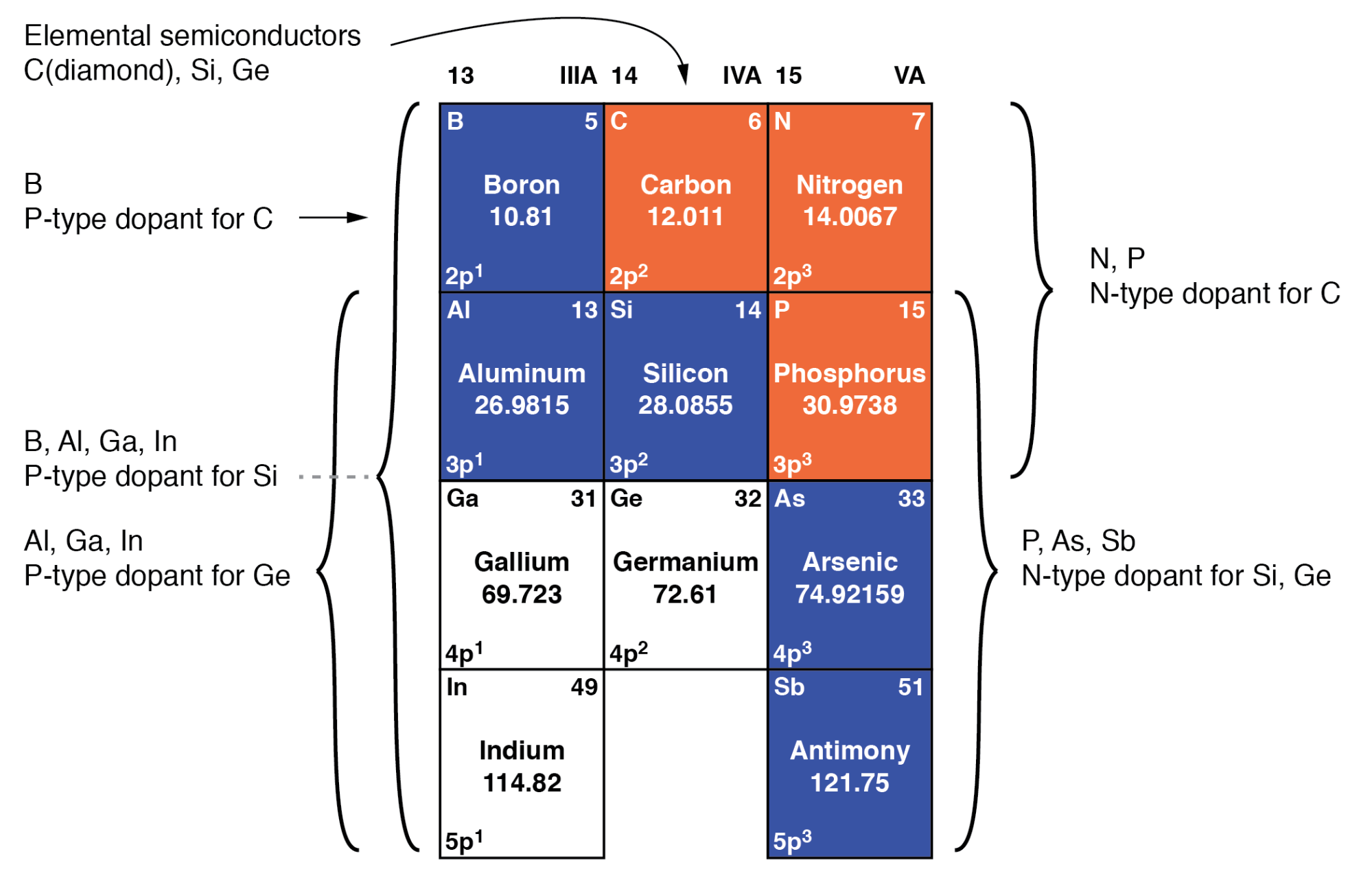
Group IIIA P‑type dopants, group IVA base semiconductors, and group VA N‑type dopants.
Silicon remains the workhorse of the industry, accounting for roughly 90 % of commercial production. Germanium is largely obsolete, while diamond is an emerging research platform. Compound semiconductors such as silicon carbide (group IVA) and gallium arsenide (group III‑V) are widely used in power electronics and optoelectronics. The table also lists III‑VI compounds (AlN, GaN, InN, etc.) and other II‑VI materials.
- Intrinsic semiconductor purity: 1 part in 10 billion → poor conductor.
- N‑type doping: pentavalent impurity → free electrons dominate → high conductivity.
- P‑type doping: trivalent impurity → excess holes dominate → high conductivity.
- Silicon is the predominant element; germanium is near‑obsolete; carbon (diamond) is emerging.
- Compound semiconductors (SiC, GaAs) are extensively employed.
RELATED WORKSHEET:
- Electrical Conduction in Semiconductors Worksheet
Industrial Technology
- Decoding Numbers and Symbols in Electronics
- Valence Electrons, Crystal Structures, and Their Role in Conductivity
- Comprehensive Op-Amp Data: National Semiconductor & CA3130 Datasheets
- Understanding Conductors, Insulators, and the Science of Electron Flow
- Understanding Voltage and Current: The Foundations of Electrical Flow
- Understanding Conductors and Insulators: From Quantum Mechanics to Practical Applications
- Reducing the Environmental Footprint of Semiconductor and Electronics Production
- Navigating the Global Semiconductor Shortage: Impact and Solutions
- The Revolution of Semiconductors: A Comprehensive Introduction
- Semiconductor Evolution Unveiled: Past, Present, and Future – Expert Q&A