


Valence Electrons, Crystal Structures, and Their Role in Conductivity
Valence Electrons
Valence electrons occupy the outermost shell of an atom and dictate its chemical behavior. These electrons are responsible for ion formation and covalent bonding, which in turn determine an element’s reactivity and its ability to conduct electricity.
Conductors
Group IA elements—Li, Na, K, Cu, Ag, and Au—each possess a single valence electron. Because this electron can be donated with minimal energy, these atoms readily form positive ions and establish metallic bonds, resulting in excellent electrical conductivity.
Periodic table group IA elements: Li, Na, K, and group IB elements: Cu, Ag, Au have one electron in the outer, or valence, shell, which is readily donated. Inner shell electrons: for n=1,2,3,4; 2n2=2,8,18,32.
Insulators
Group VIIA elements—F, Cl, Br, I, and the recently discovered Fl—contain seven valence electrons. They readily accept an electron to achieve a full octet, forming negative ions. Because they do not lose electrons, these atoms are poor conductors and function as insulators.
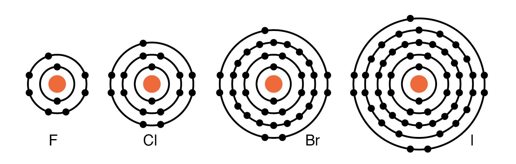
Periodic table group VIIA elements: F, Cl, Br, I with 7 valence electrons readily accept an electron in reactions with other elements.
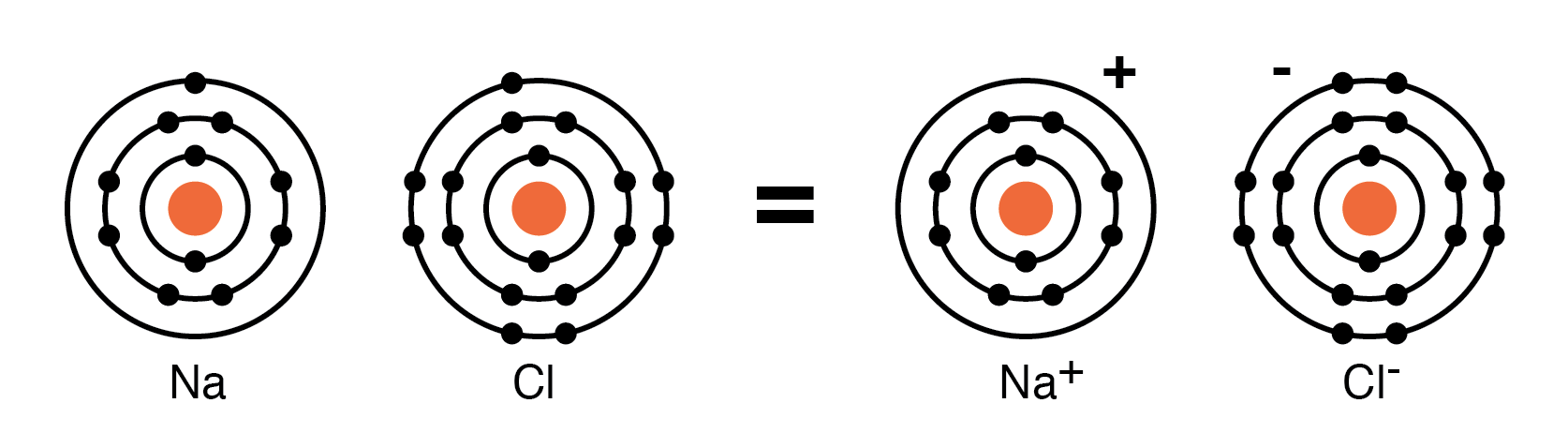
When Na donates an electron to Cl, the resulting Na+ and Cl- ions attract, forming NaCl. The crystal structure of NaCl is cubic, illustrating how charged particles can arrange into an ordered lattice.
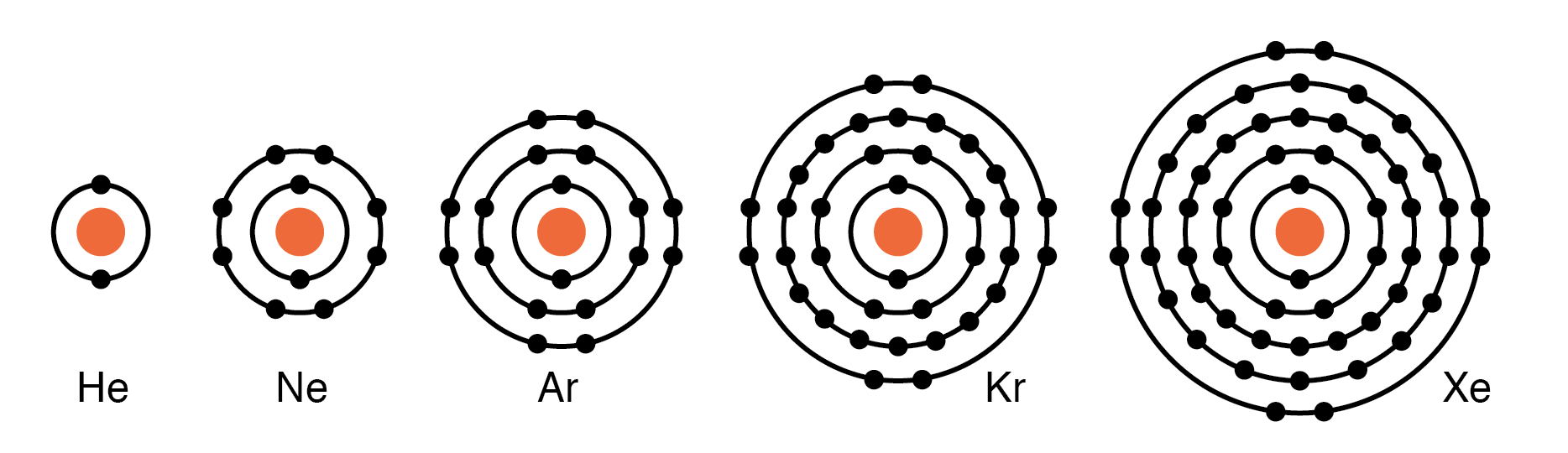
Group VIIIA elements—He, Ne, Ar, Kr, Xe—have a complete valence shell of eight electrons. Their inertness prevents them from donating or accepting electrons, rendering them excellent electrical insulators and gaseous at room temperature.
Group VIIIA elements: He, Ne, Ar, Kr, Xe are largely unreactive since the valence shell is complete.
Semiconductors
Group IVA elements—C, Si, Ge—each possess four valence electrons. These atoms share electrons with neighbors, forming covalent bonds without creating ions. The shared-electron network leads to the characteristic diamond lattice of Si and Ge, while carbon forms diamond itself.
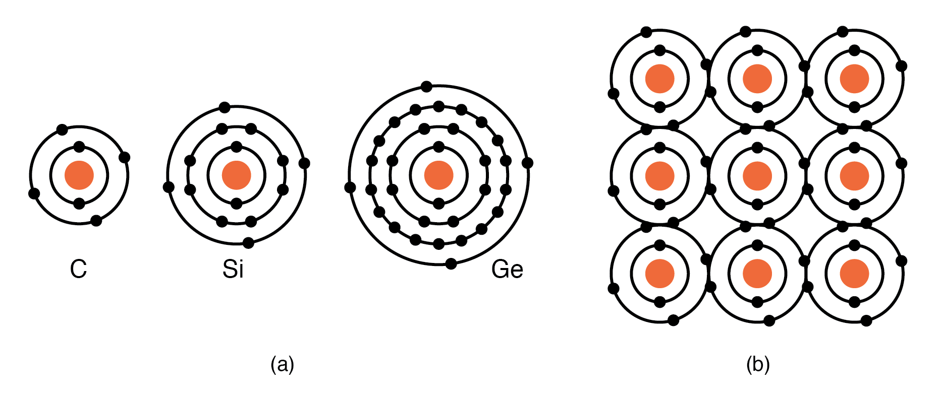
(a) Group IVA elements: C, Si, Ge having 4 electrons in the valence shell, (b) complete the valence shell by sharing electrons with other elements.
Crystal Structures
Most inorganic materials crystallize into an ordered array known as a crystal. Even metals are composed of microcrystalline grains; a polished metal sample etched with acid reveals these grains. Industrial metals are typically polycrystalline, whereas high-performance semiconductors are fabricated as single crystals (monocrystalline) to ensure uniform electrical properties.
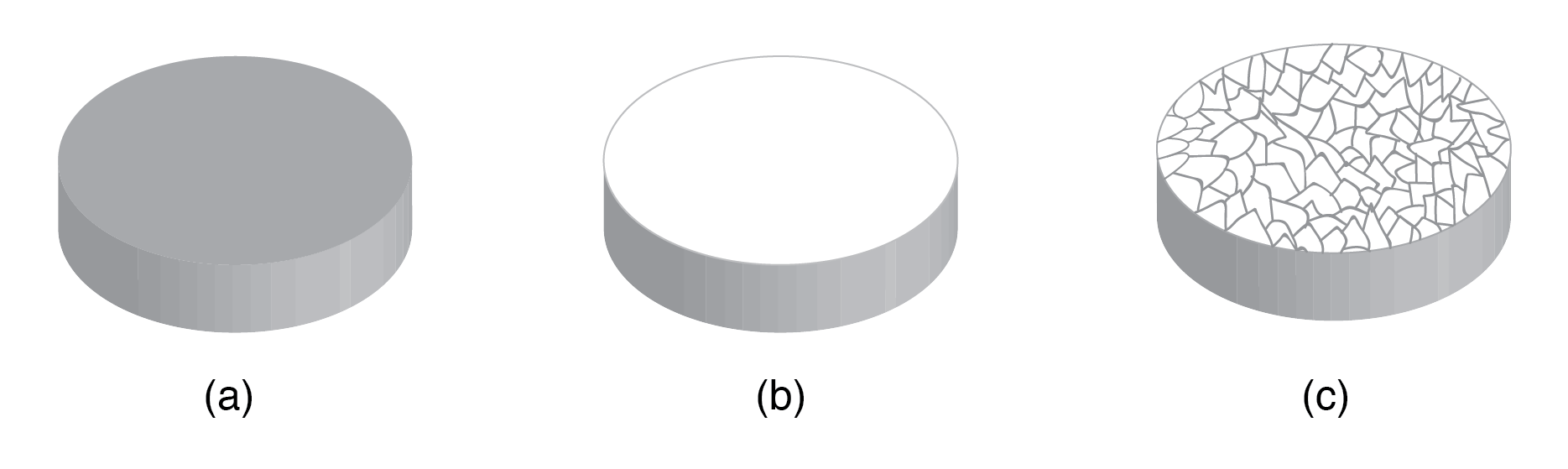
(a) Metal sample, (b) polished, (c) acid etched to show microcrystalline structure.
In ionic crystals such as NaCl, the lattice consists of alternating Na+ and Cl- ions held together by strong electrostatic forces. No free electrons are present, which is why ionic solids are poor conductors.
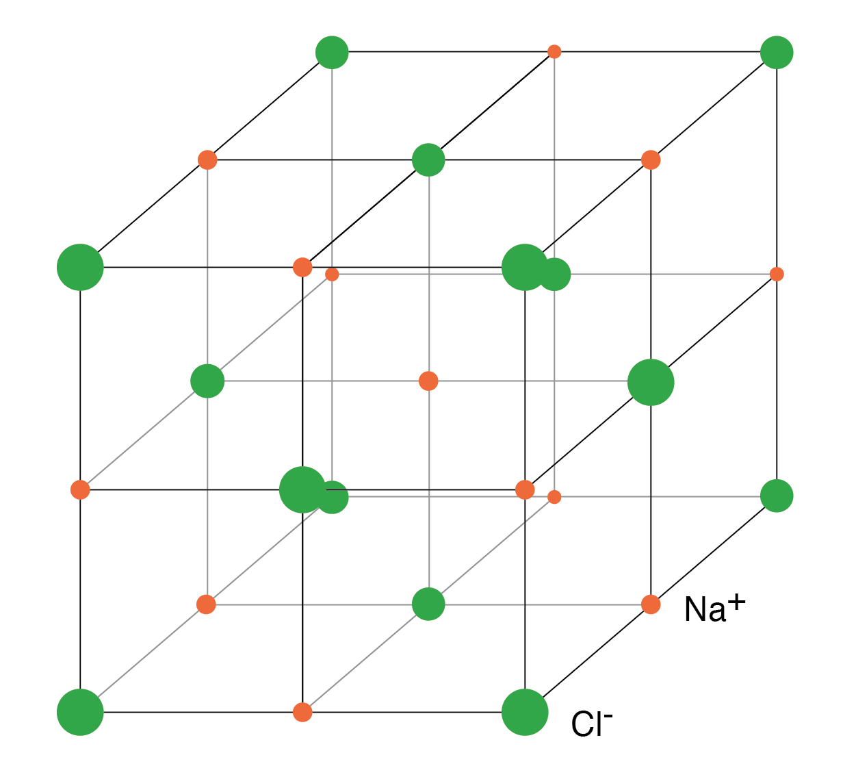
NaCl crystal having a cubic structure.
Semiconductor lattices, exemplified by Si and Ge, are built on a tetrahedral arrangement. Each atom hybridizes its one s and three p orbitals to form four sp3 orbitals, creating strong covalent bonds with four neighbors. This tetrahedral geometry gives rise to a diamond-like unit cell, which repeats throughout the crystal.
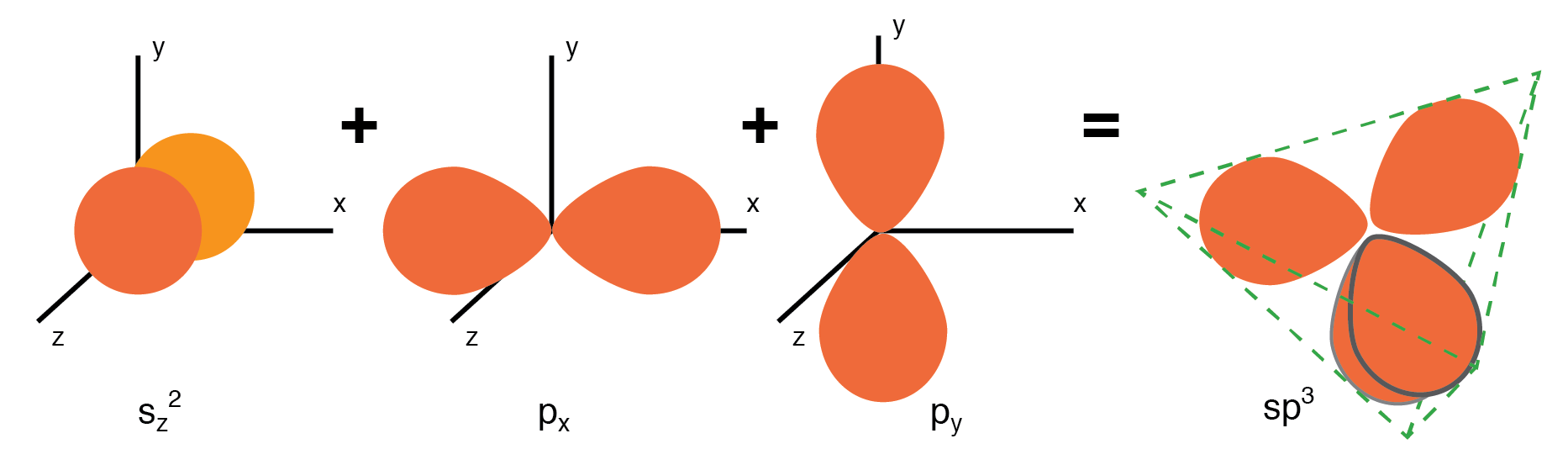
One s-orbital and three p-orbital electrons hybridize, forming four sp3 molecular orbitals.
The resulting crystal lattice is highly rigid. While free electrons are scarce, the movement of a single electron (or the creation of a hole—a missing electron) can generate significant electrical conduction, a hallmark of semiconducting behavior.
Review
- Atoms aim for a complete outer shell of eight electrons; they can donate, accept, or share electrons to achieve this.
- Atoms assemble into ordered arrays—ions or atoms—forming crystalline structures.
- Neutral atoms can become cations by donating an electron or anions by accepting one.
- Group IVA semiconductors (C, Si, Ge) crystallize into a diamond lattice, each atom covalently bonded to four neighbors.
- High-performance semiconductor devices are fabricated from single crystals.
Related Worksheet
- Electrical Conduction in Semiconductors Worksheet
Industrial Technology
- Understanding Electrons, Holes, and Doping in Semiconductors
- Understanding Conductors, Insulators, and the Science of Electron Flow
- Understanding Voltage and Current: The Foundations of Electrical Flow
- Understanding Conductors and Insulators: From Quantum Mechanics to Practical Applications
- Mastering C Structs: Passing, Returning, and Reference Handling
- Silicon Photomultipliers (SiPMs): Structure, Performance, and Key Applications
- Structures vs. Unions in C: A Practical Guide
- Impact of Morphology and Crystal Structure on Titania Nanotube Thermal Conductivity
- Designing 3D Lattice Structures: Principles, Mechanics, and Applications
- Mastering CNC Programming: Language, Structure, and G/M Codes