


Silicon Photomultipliers (SiPMs): Structure, Performance, and Key Applications
Silicon Photomultipliers: High‑Gain, Photon‑Sensitive Detectors for Modern Science and Industry
Silicon photomultipliers (SiPMs) are compact, solid‑state devices that convert single photons into measurable electrical pulses. Leveraging arrays of Geiger‑mode avalanche photodiodes (APDs), SiPMs deliver exceptional gain, nanosecond‑scale timing, and immunity to magnetic fields, making them ideal for applications ranging from medical imaging to high‑energy physics.
Why SiPMs Stand Out
- High gain (up to 106) at low bias voltages (≤ 60 V)
- Single‑photon sensitivity across 200–1100 nm wavelengths
- Fast recovery times (tens of nanoseconds) for high‑rate measurements
- Robustness to magnetic fields and mechanical shock
- Scalable design – from small micro‑cubes for UAVs to larger arrays for gamma spectroscopy
These attributes enable precise photometry, time‑of‑flight calculations, and rapid data acquisition in demanding environments.
Common Industries and Use Cases
SiPMs are now standard in:
- Biophotonics – flow cytometry, fluorescence lifetime imaging, and optical coherence tomography
- Remote sensing – LiDAR, 3D mapping, and atmospheric monitoring
- High‑energy physics – calorimetry, muon detection, and neutrino experiments
- Aerospace and defense – particle tracking, threat detection, and missile guidance
- Automotive and consumer electronics – night‑vision cameras and proximity sensors
- Oil & gas – subsea radiation monitoring and process control
Manufacturers tailor SiPMs to specific spectral windows: RGB variants for visible light and NUV types for ultraviolet detection.
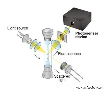
Flow cytometer application – courtesy of Hamamatsu
Internal Architecture
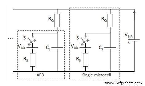
An SiPM consists of hundreds or thousands of microcells—each a self‑quenched SPAD (single‑photon avalanche diode). Each microcell contains a depletion region, a quenching resistor, and an anode–cathode pair. When biased just above breakdown voltage, a single photon triggers a Geiger‑mode avalanche that produces a current pulse proportional to the overvoltage.
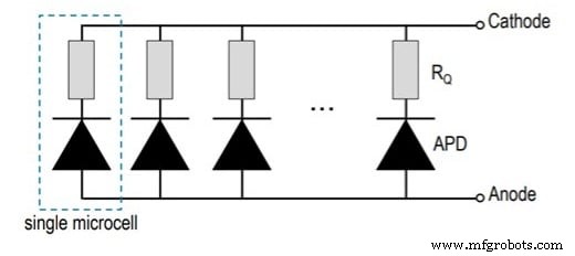
Standard SiPM structure: SPADs connected in parallel
Some vendors add a fast‑output terminal with an integrated capacitor to improve timing jitter, as shown in the SensL example.
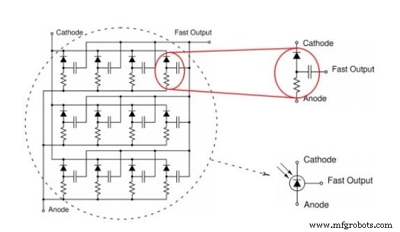
SensL fast output SiPM – courtesy of ON Semiconductor
Operating Principle
Microcells operate in Geiger mode: a photon generates an electron–hole pair that initiates an avalanche. The quenching resistor limits current, causing the junction capacitance to discharge rapidly. The microcell then recharges and returns to Geiger mode, ready for the next photon.
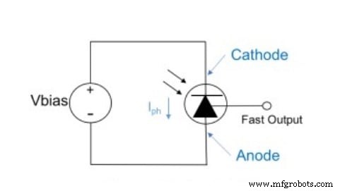
Biasing the SiPM – courtesy of ON Semiconductor
Equivalent circuit diagrams illustrate how the APD acts as a light‑activated switch: with no light, the junction capacitance holds the bias voltage; upon photon absorption, the switch closes, the capacitance discharges, and a current pulse is generated.
Equivalent circuit of a SiPM – courtesy of Hamamatsu
The pulse shape is typically a few nanoseconds wide, with an amplitude that scales linearly with overvoltage until saturation.
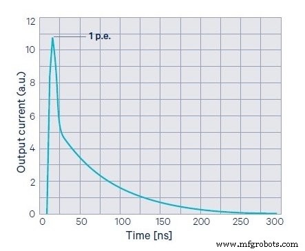
SiPM output current pulse – courtesy of First Sensor
Key Performance Parameters
Photon Detection Efficiency (PDE)
PDE measures how effectively an SiPM converts incident photons into electrical pulses. It depends on overvoltage, wavelength, and microcell geometry. Typical PDE values range from 20% to 50% across the visible spectrum.
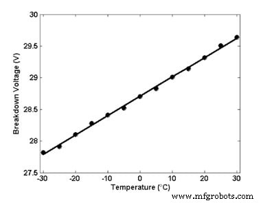
Breakdown Voltage and Overvoltage
Breakdown voltage (VBD) is the minimum reverse bias needed for avalanche multiplication. The operating bias (VBIAS) is set above VBD by an overvoltage ΔV, which boosts PDE and gain but also increases dark counts and afterpulsing. Temperature variations shift VBD, so temperature‑compensated biasing is common.
Recovery Time
The recovery time, governed by the quenching resistor and junction capacitance (RQCJ), is the interval between quenching and full readiness for the next photon. Typical recovery times are 20–50 ns, allowing SiPMs to handle photon rates up to several MHz per pixel.
Temperature Dependence
Higher temperatures increase VBD, reduce PDE, and raise dark count rates (often doubling per 10 °C). Proper thermal management or temperature‑controlled biasing mitigates these effects.
Noise Sources
Noise in SiPMs originates from two main mechanisms:
- Dark counts – thermally generated carriers causing avalanches in the absence of light.
- Correlated noise – afterpulsing and optical crosstalk triggered by a primary avalanche.
Afterpulsing
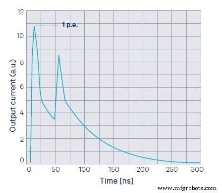
Trapped carriers released during recovery generate secondary pulses of lower amplitude. The probability is proportional to overvoltage and trap density.
Optical Crosstalk
Secondary photons emitted during an avalanche can trigger adjacent microcells, increasing pulse amplitude and complicating photon‑counting. Crosstalk rises with overvoltage and can reach 20–30% in some devices.
Conclusion
SiPMs combine the high sensitivity of traditional photomultipliers with the robustness and scalability of solid‑state technology. While noise and temperature sensitivity remain challenges, ongoing material and circuit innovations continue to push PDE, timing, and dynamic range to new heights. As these devices mature, their adoption across scientific, industrial, and consumer sectors is set to accelerate dramatically.
Industrial Technology
- Titanium: Key Properties and Real‑World Applications
- Titanium Valves: Properties, Performance, and Key Applications
- Tantalum Capacitors: Key Characteristics & Applications
- Molybdenum and Its Alloys: Key Applications in Material Processing
- Hafnium Oxide (HfO₂): Structure, Properties, and Key Applications
- Fiberglass Adhesive Tape: High‑Temperature Resistance & Versatile Applications
- Electronic Structure and Transport in InSe Nanoribbons: Edge Effects and Hydrogen Passivation
- Artificial Intelligence: Evolution, History, and Real-World Applications
- Mastering Microcontrollers: Structure, Functionality, and Practical Applications
- Applications & Characteristics of DC Motors: Performance, Efficiency, and Versatility