


Junction Field‑Effect Transistors (JFET): Design, Operation, and Advanced Variants
The field‑effect transistor concept dates back to Julius Lilienfeld’s 1926 and 1933 U.S. patents (1,900,018). In 1947, Shockley, Brattain, and Bardeen explored the device, but practical hurdles redirected them toward the bipolar transistor. Shockley’s seminal theory appeared in 1952, yet only in 1960 did John Atalla fabricate a working JFET, marking a milestone in semiconductor processing.
A field‑effect transistor (FET) is a unipolar device that conducts current using a single type of charge carrier. An N‑type slab hosts electrons, whereas a P‑type slab carries holes.
FET Operation
At the circuit level, the gate voltage governs the channel resistance between source and drain. In an N‑channel device, the channel is a lightly doped N‑type silicon slab; the heavily doped P‑type regions on either side form the gate, analogous to the base of a BJT. The source and drain terminals correspond to the emitter and collector, respectively.
Manufacturing FETs demands a clean‑room environment. Even minor contamination can compromise the device, making fabrication more challenging than for bipolar transistors. Today, most integrated circuits employ metal‑oxide‑semiconductor (MOS) FETs, but discrete JFETs remain in use.
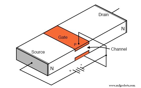
Junction field‑effect transistor cross‑section.
In a properly biased N‑channel JFET, the gate forms a reverse‑biased diode junction with the source‑drain slab. When a voltage is applied between source and drain, the lightly doped N‑type channel conducts in either direction—no gate bias is needed for conduction. However, applying a reverse bias to the gate expands the depletion region, increasing the channel resistance. The gate voltage at which the channel pinches off is called the pinch‑off voltage (V_P), typically a few volts.
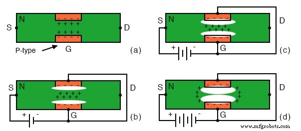
Figure 1 illustrates how the depletion region grows as reverse bias increases: (a) initial depletion, (b) moderate bias enlarges the depletion region, (c) higher bias narrows the channel, and (d) pinch‑off occurs, dramatically raising resistance.
Source and drain are interchangeable, allowing current to flow in either direction for low drain voltages (<0.6 V). For higher drain supplies (tens of volts), the depletion region extends toward the drain, slightly increasing channel resistance. The schematic symbol for an N‑channel FET is shown below, with the gate arrow indicating the diode‑like junction.
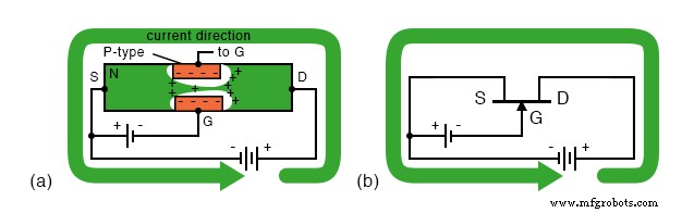
N‑channel JFET: cross‑section (a) and schematic symbol (b). The arrow points in the same direction as a junction diode. The non‑pointing bar denotes N‑type material.
In a P‑channel device, the roles reverse: the channel is P‑type, the gate is heavily doped N‑type, and all voltage polarities flip relative to the N‑channel configuration. The schematic arrow points outward from the gate.
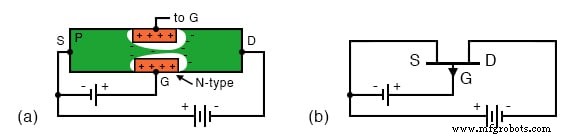
P‑channel JFET: (a) cross‑section, (b) schematic symbol. Increasing positive gate bias raises resistance, reducing drain current.
Discrete JFETs are fabricated with the gate positioned on the wafer’s top surface, heavily doped P⁺ to provide a wide depletion region, and heavily doped N⁺ source/drain to minimize contact resistance. The lightly doped N⁻ channel allows deep penetration of gate‑induced depletion.
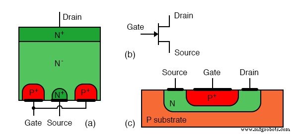
JFET device cross‑sections: (a) discrete device, (b) schematic symbol, (c) integrated‑circuit layout.
Integrated‑circuit FETs expose all three terminals on the die surface, enabling metalization layers to interconnect multiple devices. For high‑frequency analog applications, the channel beneath the gate is made very thin, eliminating the need for gate regions on both sides.
Static Induction Transistor (SIT)
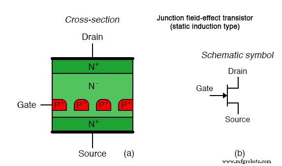
SITs are short‑channel, buried‑gate devices designed for power handling. They feature low gate resistance and minimal gate‑to‑source capacitance, allowing rapid switching. SITs can deliver hundreds of amps, thousands of volts, and reach frequencies up to 10 GHz.
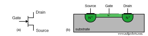
Metal‑Semiconductor FET (MESFET)
MESFETs resemble JFETs but use a Schottky metal contact as the gate instead of a junction diode. The Schottky gate provides lower capacitance and higher speed. MESFETs are depletion‑mode devices (normally on) and are employed as microwave power amplifiers up to 30 GHz. They can be fabricated on silicon, gallium arsenide, indium phosphide, silicon carbide, and diamond.
Key Takeaways
- JFETs are unipolar devices; channel conduction relies on a single carrier type.
- The gate’s reverse bias controls channel resistance via depletion region expansion.
- Source, gate, and drain map directly onto BJT emitter, base, and collector.
- Advanced variants—SIT and MESFET—extend JFET principles to high‑power and high‑frequency applications.
Further Learning
- Junction Field‑Effect Transistors (JFET) Worksheet
Industrial Technology
- Understanding Junction Field-Effect Transistors (JFETs): Gate Current Direction & N‑Channel vs P‑Channel
- Transistors: IGFET (MOSFET) – Depletion & Enhancement Modes Explained
- CMOS Gate Circuits: Design, Operation, and Comparison to TTL
- Understanding Bipolar Junction Transistors: Structure, Operation, and Amplification
- Insulated‑Gate Field‑Effect Transistors (MOSFETs) – Design, Operation, and Power Variants
- Bipolar Junction Transistors (BJT): Core Principles and Practical Applications
- Understanding Junction Field‑Effect Transistors (JFET): Fundamentals and Applications
- Using a Junction Field‑Effect Transistor (JFET) as a Low‑Power On/Off Switch
- Understanding Insulated‑Gate Field‑Effect Transistors (IGFETs)
- Field-Effect Transistor Biosensors Deliver High Sensitivity and Real-Time Detection Across Healthcare, Food Safety, and Environmental Monitoring