


Understanding Bipolar Junction Transistors: Structure, Operation, and Amplification
History and Origin
The bipolar junction transistor (BJT) earned its name from the simultaneous conduction of electrons and holes within a single crystal. The first practical BJT was invented at Bell Labs by William Shockley, Walter Brattain, and John Bardeen in late 1947 and published in 1948. The trio received the 1956 Nobel Prize in Physics for this breakthrough.
Basic Structure of an NPN BJT
An NPN transistor consists of three layers: an heavily doped N‑type emitter, a thin P‑type base, and a lightly doped N‑type collector. Think of it as a second layer added to a diode. The critical design element is the base thickness – it must be thin enough to allow most carriers to diffuse through without recombining, yet thick enough to prevent electrical shorting between emitter and collector.
BJT Junctions and Biasing
Every transistor has two p‑n junctions: emitter‑base (EB) and base‑collector (BC). In a typical amplifier configuration, the EB junction is forward‑biased while the BC junction is reverse‑biased. The reverse bias widens the BC depletion region, creating a strong electric field that sweeps minority carriers from the base into the collector. The EB junction requires a forward voltage of roughly 0.6 V (silicon) to inject majority carriers from the emitter into the base as minority carriers.
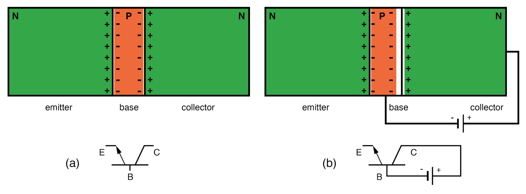
Figure 1. (a) NPN transistor cross‑section. (b) Reverse‑biased BC junction increases depletion width; negligible current flows except for leakage.
Current Amplification Mechanism
When the EB junction is forward‑biased, electrons from the emitter enter the P‑type base as minority carriers. The thin base allows most of these electrons to reach the depletion region at the BC junction before recombining. Once inside the depletion region, the strong electric field pulls them into the collector, producing a large collector current. The small base current that does flow controls the majority of the collector current, giving rise to the transistor’s current gain.
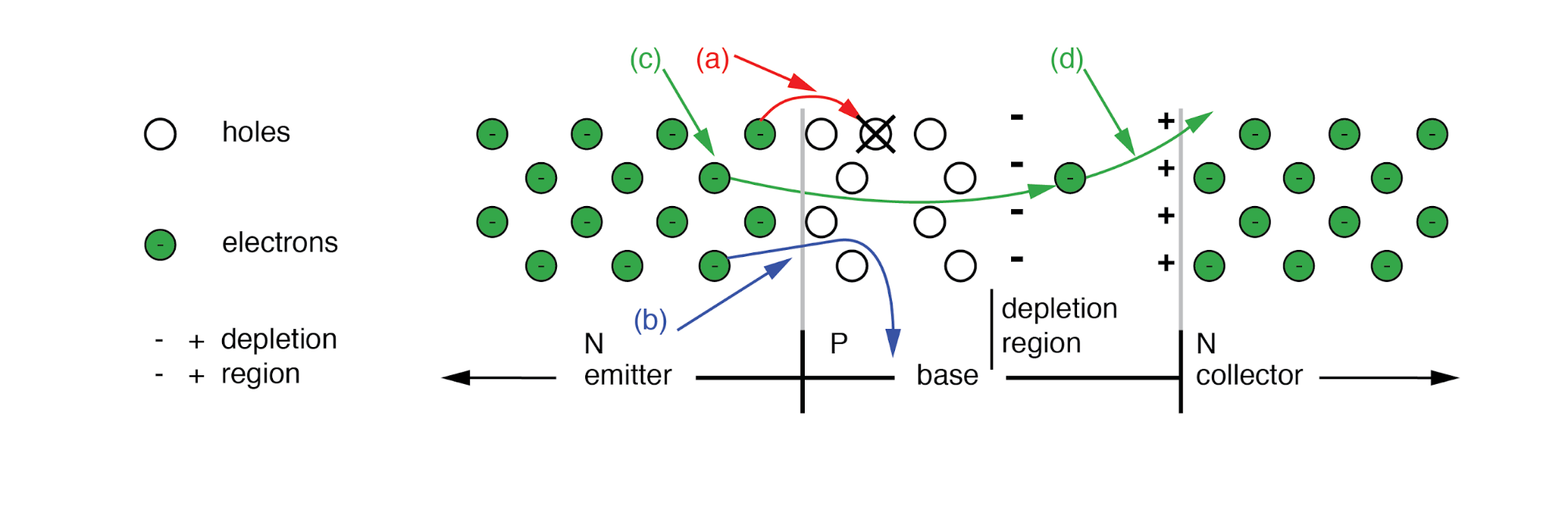
Figure 2. Electron fates in the base: (a) recombination with holes, (b) exit via base lead, (c) diffusion through base to collector, (d) swept into collector by the BC field.
The emitter efficiency (α) – the ratio IC/IE – typically reaches 0.99 for small‑signal silicon BJTs, meaning 99 % of injected electrons reach the collector. The current gain (β = IC/IB) usually falls between 100 and 300 for these devices.
PNP vs NPN Transistors
Both NPN and PNP transistors operate on the same principle but with opposite carrier types and bias directions. The arrow on the emitter symbol indicates the direction of conventional current flow: away from the base for NPN, toward the base for PNP. The base‑collector junction polarity is the same as the base‑emitter junction, but the supply polarities are reversed.
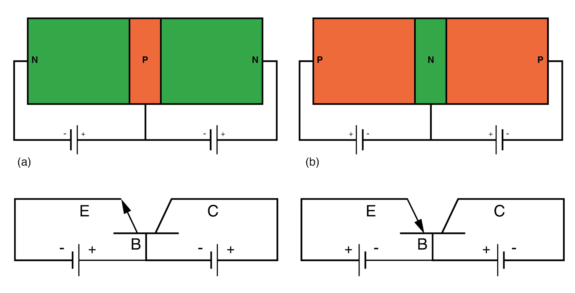
Figure 3. (a) NPN transistor schematic. (b) PNP transistor schematic.
Device Fabrication and Packaging
On a semiconductor die, the emitter is heavily doped (N+), the base is lightly doped (P), and the collector is lightly doped near the base but heavily doped at the metal contact to reduce resistance. Small‑signal BJTs typically have a collector‑base breakdown voltage of 60–80 V, while high‑voltage variants can exceed several hundred volts. In power packages, the collector is often bonded to the metal case for efficient heat dissipation.
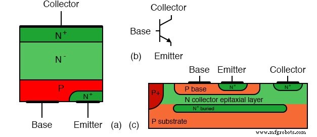
Figure 4. (a) Discrete BJT cross‑section. (b) Schematic symbol. (c) Integrated circuit cross‑section.
Key Takeaways
- BJTs conduct current using both electrons and holes.
- Amplification requires a forward‑biased EB junction and a reverse‑biased BC junction.
- Unlike back‑to‑back diodes, the base is extremely thin, allowing carrier diffusion to the collector.
- Emitter efficiency (α) ≈ 0.99 for small‑signal devices.
- Current gain (β) ranges from 100 to 300 in small‑signal BJTs.
Related Worksheets
Industrial Technology
- Bipolar Transistors: Symbols, Types, and Applications
- Understanding Junction Field-Effect Transistors (JFETs): Gate Current Direction & N‑Channel vs P‑Channel
- Hybrid Transistor Design: IGFET‑BJT Combo for High Gain and Low Drop
- CMOS Gate Circuits: Design, Operation, and Comparison to TTL
- Understanding Bipolar Junction Transistors: Structure, Operation, and Amplification
- Junction Field‑Effect Transistors (JFET): Design, Operation, and Advanced Variants
- Bipolar Junction Transistors (BJT): Core Principles and Practical Applications
- BJT Switching: How Transistors Efficiently Control High‑Current Loads
- Understanding Junction Field‑Effect Transistors (JFET): Fundamentals and Applications
- Thermocouples: Harnessing the Seebeck Effect for Accurate Temperature Measurement