


CMOS Gate Circuits: Design, Operation, and Comparison to TTL
Up until this point, our analysis of transistor logic circuits has been limited to the TTL design paradigm, whereby bipolar transistors are used, and the general strategy of floating inputs being equivalent to “high” (connected to Vcc) inputs—and correspondingly, the allowance of “open‑collector” output stages—is maintained. This, however, is not the only way we can build logic gates.
Field‑Effect Transistors
Field‑effect transistors, particularly the insulated‑gate variety, can be employed in gate design. Because they are voltage‑controlled rather than current‑controlled, IGFETs enable simpler circuitry. Consider the inverter shown below, built with P‑ and N‑channel IGFETs:
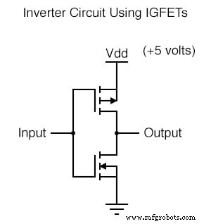
The label Vdd on the positive supply follows the same convention as Vcc in TTL: it denotes the constant voltage applied to the drain of a field‑effect transistor, referenced to ground.
Gate Operation with Enhancement‑Mode IGFETs
Low Input
Connect the circuit to a power source and input switch and observe its behavior. Note that these IGFETs are E‑type (enhancement‑mode) and thus normally off.
They turn on only when the gate‑to‑drain (or gate‑to‑substrate) voltage has the correct polarity.
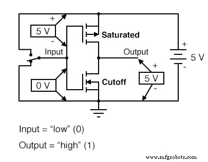
The upper transistor is P‑channel. When its substrate is more positive than the gate (gate negative relative to substrate), the channel enhances and current flows between source and drain. In the illustration, the top transistor is on, while the lower N‑channel transistor is off (zero gate‑to‑substrate voltage).
Consequently, the output connects firmly to Vdd and has a very high resistance to ground, yielding a logical “high” (1) when the input is “low” (0).
High Input
Switch the input to the opposite state:
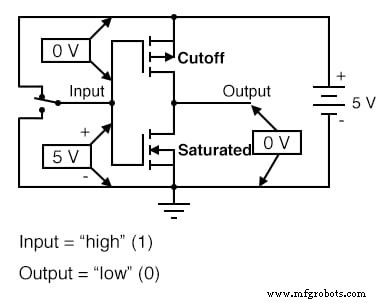
Now the lower N‑channel transistor saturates, while the upper P‑channel remains off. The output becomes “low” (0). The circuit functions as an inverter (NOT gate).
Complementary Metal‑Oxide‑Semiconductors (CMOS)
Using MOSFETs instead of bipolar transistors greatly simplifies inverter design. The output never floats—thanks to the natural “totem‑pole” configuration that can both source and sink load current.
The elegance of this gate stems from the complementary use of P‑ and N‑channel IGFETs. Such circuits are classified as CMOS (Complementary Metal‑Oxide‑Semiconductor).
Challenges and Solutions in CMOS Gates
Unlike TTL, CMOS gates are susceptible to high voltages from static electricity and can be inadvertently driven into a logic state if left floating. Therefore, floating inputs should always be avoided.
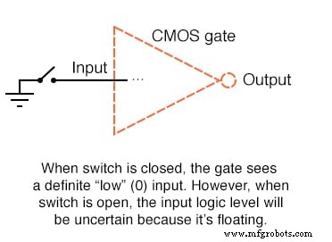
Floating‑Input Problems
Consider a single‑throw switch that connects an input to Vdd or ground in one state, but leaves it floating in the other:
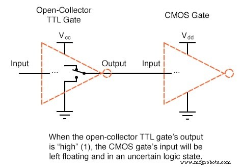
Similarly, an open‑collector TTL output (which floats when high) can leave a CMOS input undefined:
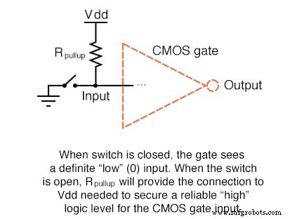
Pull‑Up and Pull‑Down Resistors
To stabilize floating inputs, a resistor is connected to Vdd (pull‑up) or ground (pull‑down). A typical value is 10 kΩ, though the exact resistance is not critical.
Pull‑up example:
Pull‑down example:
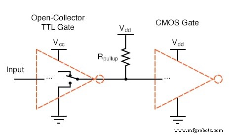
When interfacing an open‑collector TTL output to a CMOS input, a pull‑up resistor is required to define the high state:
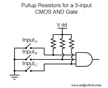
For multi‑input CMOS gates, each input requires its own pull‑up or pull‑down resistor.
Designing Multi‑Input CMOS Gates
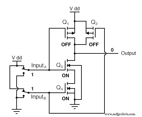
CMOS NAND Gate
Below is a typical CMOS NAND schematic:
Transistors Q1 and Q3 form a series P‑/N‑channel pair controlled by input A, while Q2 and Q4 form a similar pair for input B. The upper transistors source current from Vdd, the lower transistors sink to ground. The output is high unless both lower transistors conduct simultaneously, i.e., only when both inputs are high.
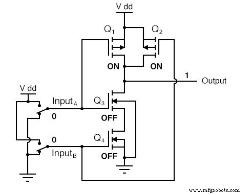
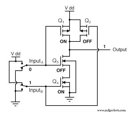
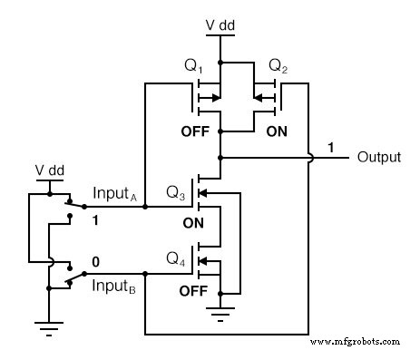
Truth Table Illustrations
Below are visual depictions of the NAND gate’s behavior for all four input combinations:
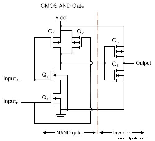
CMOS AND Gate
An AND gate can be obtained by inserting an inverter stage at the output of a NAND gate:
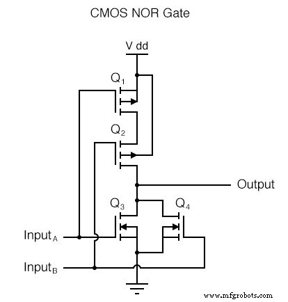
CMOS NOR Gate
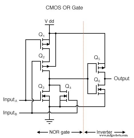
Similar to the NAND, a NOR gate uses four MOSFETs but arranges them differently: two series sourcing transistors and two parallel sinking transistors. The output goes high only when both inputs are low.
CMOS OR Gate
By adding an inverter to a NOR gate’s output, an OR function is achieved.
TTL vs. CMOS: Pros and Cons
Both TTL and CMOS can implement any logical function, yet they differ significantly in key aspects:
- Power Consumption: CMOS draws virtually no static current, whereas TTL consumes a constant bias current. However, CMOS power rises with switching frequency; TTL power remains relatively constant.
- Fan‑Out: CMOS inputs draw minimal current, enabling a single gate to drive many others. TTL fan‑out is limited by current‑controlled inputs.
- Supply Voltage Range: TTL typically operates at 4.75–5.25 V. CMOS comfortably spans 3–15 V, owing to its voltage‑controlled MOSFETs.
- Speed: TTL generally outpaces CMOS because MOSFET input capacitance introduces larger RC time constants, slowing rise/fall times.
Enhancing CMOS Speed: B‑Series Gates
To mitigate CMOS’s slower response, output buffers (two cascaded inverters) can be added, increasing voltage gain and speeding up transitions. Although logically redundant, the additional stages improve performance by amplifying signal swings.
Review
- CMOS logic gates use MOSFETs instead of bipolar transistors.
- Inputs are sensitive to static electricity and must not float.
- Pull‑up/pull‑down resistors resolve floating‑input issues.
- CMOS consumes less power than TTL, but power rises with frequency.
- CMOS inputs draw far less current, allowing higher fan‑out.
- CMOS operates over a wider supply range (3–15 V) versus TTL (4.75–5.25 V).
- CMOS has a lower maximum frequency due to input capacitance.
- B‑Series gates use buffered outputs to improve speed.
Related Worksheets
- Insulated Gate Field‑Effect Transistors Worksheet
- CMOS Logic Gates Worksheet
Industrial Technology
- Designing and Verifying a Basic NAND Gate Circuit with the 4011 IC
- Bipolar Transistors: Symbols, Types, and Applications
- Understanding Junction Field-Effect Transistors (JFETs): Gate Current Direction & N‑Channel vs P‑Channel
- Transistors: IGFET (MOSFET) – Depletion & Enhancement Modes Explained
- Hybrid Transistor Design: IGFET‑BJT Combo for High Gain and Low Drop
- CMOS Gate Circuits: Design, Operation, and Comparison to TTL
- Gate Universality: Replicating Any Logic Function with NAND or NOR Gates
- Junction Field‑Effect Transistors (JFET): Design, Operation, and Advanced Variants
- Insulated‑Gate Field‑Effect Transistors (MOSFETs) – Design, Operation, and Power Variants
- Thyristors: Types, Operation, and the Power of Silicon Controlled Rectifiers (SCRs)