


Understanding TTL NOR and OR Gates: Circuit Analysis and Conversion
TTL Circuit Analysis
Let’s analyze a classic TTL NOR gate and see how it can be transformed into an OR gate. The circuit below illustrates the key components:
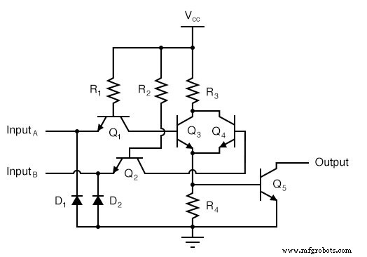
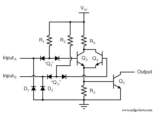
Transistors Q1 and Q2 serve as two‑diode steering networks, much like the steering network used in other TTL designs. Replacing them with explicit diodes makes the operation clearer:
When input A is left floating or tied to Vcc, base current flows into Q3, driving it into saturation. If A is grounded, that current is diverted through the left steering diode of the equivalent “Q1,” forcing Q3 into cutoff. The same logic applies to input B and transistor Q4.
Notice that Q3 and Q4 share collector and emitter nodes, effectively acting as parallel switches. If either input is high, one of the transistors saturates, allowing current to flow through resistors R3 and R4 and turning on the output transistor Q5 to a low logic level. The output becomes high only when both Q3 and Q4 are cut off, which occurs when both inputs are low.
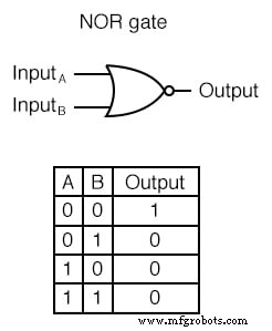
Thus the circuit implements a NOR gate, as confirmed by its truth table:
To convert this NOR gate into an OR gate, we simply add an inverter stage at the output—mirroring the approach used to turn NAND into AND:
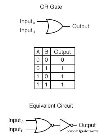
The resulting truth table for the OR gate is:
Both NOR and OR TTL circuits can also employ totem‑pole output stages for improved drive capability.
Review:
- Adding an inverter to the NOR output yields a functional OR gate.
Industrial Technology
- Designing and Verifying a Basic NAND Gate Circuit with the 4011 IC
- NOR Gate SR Latch: Building and Understanding Digital Memory
- Building an Enabled NAND‑Gate SR Latch: Parts, Design, and Operation
- Essential DC Circuit Equations and Laws for Engineers
- Understanding Multiple-Input Logic Gates: Functions, Truth Tables, and Practical Applications
- TTL NAND and AND Gate Implementation Using Open‑Collector Transistor Circuits
- Special-Output Logic Gates: Complementary, Tristate, and Bilateral Switches
- Gate Universality: Replicating Any Logic Function with NAND or NOR Gates
- Mastering Series RLC Circuit Analysis: From Impedance to KVL
- Understanding Q Factor and Bandwidth in Resonant Circuits: Theory, Calculations, and Practical Design