


Special-Output Logic Gates: Complementary, Tristate, and Bilateral Switches
Complementary Output Gates
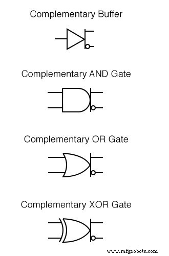
In many designs, engineers need a gate that delivers both inverted and non‑inverted outputs from a single logic element. A classic example is a one‑input buffer that also acts as an inverter, providing separate terminals for each function.
Two‑input gates that simultaneously deliver AND and NAND results are also available. These devices are called complementary output gates.
The standard symbol for such a gate is the basic gate shape with a bar and two output lines. An array of complementary symbols is shown below:
Benefits of Complementary Gates
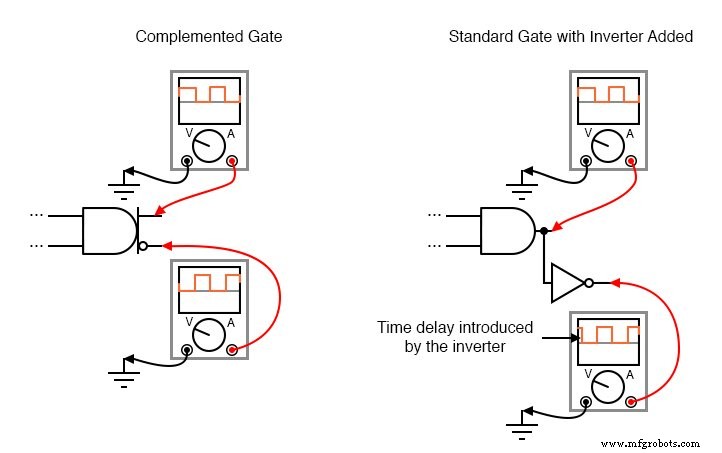
Complementary gates are invaluable in dense circuitry where space is at a premium. They eliminate the need for extra inverter ICs, saving board real estate and reducing component count.
Because the inverted and non‑inverted outputs switch almost simultaneously, there is no significant propagation delay between them. This property is critical in timing‑sensitive applications.
Tristate Gates
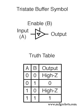
Tristate outputs can assume three distinct states: driving a logic low (current sink), driving a logic high (current source), or remaining floating (high‑impedance). They are commonly added to buffer gates via an extra control pin called the enable.
When the enable is high (logic 1), the buffer behaves like a normal push‑pull stage. When the enable is low (logic 0), the output goes to high‑Z, effectively disconnecting the gate from the circuit.
In schematic notation, a tristate buffer is indicated by a triangle inside the gate symbol:
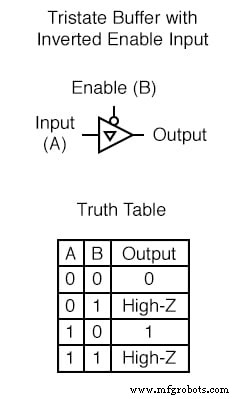
Some manufacturers provide an inverted‑enable version, where the high‑Z state occurs when the enable is high:
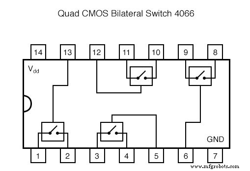
Bilateral Switches
Bilateral switches are solid‑state SPST devices built from MOSFETs. In the ON state, their resistance is only a few hundred ohms; in the OFF state, the resistance rises to several hundred megaohms.
These switches appear in schematics as a rectangle with a control pin and two terminals, much like a relay but without moving parts. Because they are semiconductor devices, they avoid mechanical issues such as bouncing, arcing, and vibration.
However, bilateral switches have limited current handling, and the signal voltage must stay within the supply rails of the switch IC.
The 4066 IC contains four independent bilateral switches:
Quick Review
- Complementary gates deliver inverted and non‑inverted outputs with negligible delay.
- Tristate gates offer high, low, and high‑Z outputs, controlled by an enable pin.
- Bilateral switches are solid‑state relays that can switch analog or digital signals, but with modest current capability.
Related Worksheet
- Boolean Algebra Worksheet
Industrial Technology
- Designing and Verifying a Basic NAND Gate Circuit with the 4011 IC
- Building an Enabled NAND‑Gate SR Latch: Parts, Design, and Operation
- Understanding the Buffer Gate: Amplification and Signal Integrity in Digital Circuits
- Understanding Multiple-Input Logic Gates: Functions, Truth Tables, and Practical Applications
- TTL NAND and AND Gate Implementation Using Open‑Collector Transistor Circuits
- Understanding TTL NOR and OR Gates: Circuit Analysis and Conversion
- Gate Universality: Replicating Any Logic Function with NAND or NOR Gates
- Thyristors: Types, Operation, and the Power of Silicon Controlled Rectifiers (SCRs)
- Six Injection Molding Gate Types and How to Choose the Right One
- The Definitive Guide to Logic Gate Truth Tables