


TTL NAND and AND Gate Implementation Using Open‑Collector Transistor Circuits
By adding a second input to a standard open‑collector TTL inverter, we obtain a circuit that naturally implements a NAND function. In this article we walk through the analysis, explain the underlying transistor behavior, and show how a simple inverter can be turned into an AND gate by adding one more inverter stage.
From Inverter to Two‑Input Device
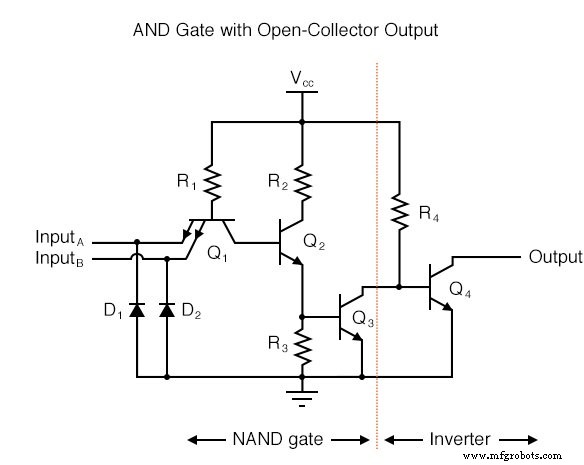
Our starting point is a conventional open‑collector TTL inverter. The circuit is extended by connecting a second input terminal to the base of the second transistor, Q2, exactly as the first input is connected. The resulting schematic looks like this:
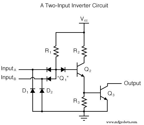
Although the diagram is simple, the device does not function as a “two‑input inverter.” Through logical analysis we will determine its truth table and give it the proper designation.
Transistor Structure
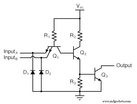
The “steering” diode cluster marked Q1 is effectively a transistor that is not used for amplification. A standard NPN transistor cannot provide the three PN junctions needed in this network, so we use a transistor with one collector, one base, and two emitters. In the circuit it is drawn as follows:
Input States and Output Behavior
With a single input, grounding the input forces the output high (floating), while allowing the input to float or tie to Vcc pulls the output low. When two inputs are added, each behaves identically. If either input is grounded, transistor Q2 cuts off, Q3 remains off, and the output floats high. Only when both inputs are high does Q2 saturate, Q3 turns on, and the output pulls low.
Illustrations of the three key states:
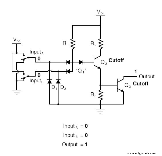
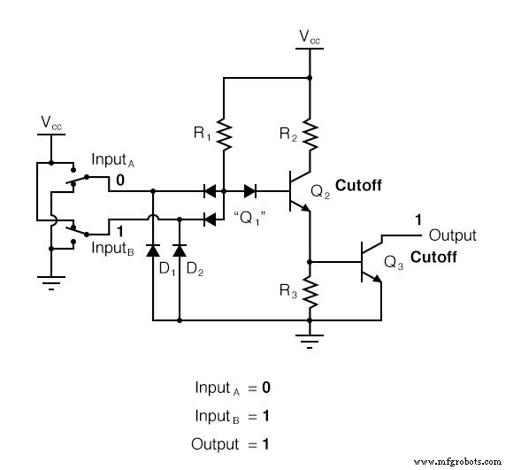
In each case, a grounded input guarantees a high output. The only scenario where the output goes low is when both inputs are high, which forces Q2 into saturation and Q3 to conduct.
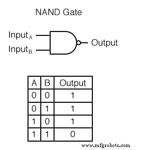
NAND Gate
Tabulating these results yields the standard NAND truth table:
Thus, a TTL NAND gate is the simplest, most natural function of this open‑collector design. In earlier sections we described a NAND gate as an AND gate followed by an inverter. Here we see that the same circuit already embodies the NAND behavior without extra complexity.
Creating an AND Gate
To obtain an AND function we simply add an inverter stage to the output of the NAND circuit, just as we add a transistor stage to a TTL inverter to make a buffer:
The resulting truth table and schematic are shown below:
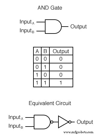
Both NAND and AND gates can also be implemented with totem‑pole outputs instead of open‑collector. For simplicity, we present the open‑collector versions here.
Key Takeaways
- Adding a second input to a TTL inverter yields a NAND gate.
- An AND gate is obtained by inserting an inverter after the NAND output.
Related Resources
Industrial Technology
- Building an Enabled NAND‑Gate SR Latch: Parts, Design, and Operation
- Essential DC Circuit Equations and Laws for Engineers
- Understanding TTL NOR and OR Gates: Circuit Analysis and Conversion
- Special-Output Logic Gates: Complementary, Tristate, and Bilateral Switches
- Input & Output Coupling Techniques for Amplifiers: Capacitive, Direct, and Transformer Methods
- Mastering Series RLC Circuit Analysis: From Impedance to KVL
- Understanding Q Factor and Bandwidth in Resonant Circuits: Theory, Calculations, and Practical Design
- Mastering Input and Output in C Programming
- Flex Circuit Materials and Construction: Building Durable, High-Performance PCBs
- High‑Performance Variable Voltage & Current Power Supply – Stable Output for Lab and Industrial Use