


Understanding the Buffer Gate: Amplification and Signal Integrity in Digital Circuits
When two inverter gates are cascaded—output of one feeding the input of the second—the two inversions cancel, producing a non‑inverting path. Though this might appear redundant, it serves a critical role: amplifying weak signals.
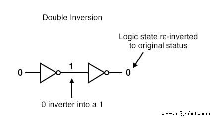
In TTL logic, every gate acts as a signal amplifier. A weak source that can’t source or sink sufficient current is boosted by the pair of inverters. The logic level stays the same, but the final inverter’s full current‑sourcing and sinking capability is available to drive the subsequent load.
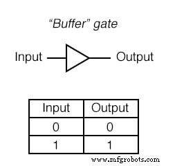
A dedicated component, the buffer gate, performs exactly this function. Its symbol is a triangle without the inverting “bubble” on the output terminal:
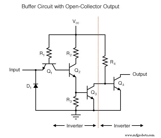
Buffer circuits can be built with either open‑collector or totem‑pole output stages. A typical open‑collector buffer adds one more common‑emitter transistor to re‑invert the signal.
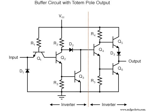
High‑Input Analysis
With a logic‑high input, the left steering diode of Q1 remains reverse‑biased, so R1’s current feeds the base of Q2, driving it into saturation. Saturated Q2 forces Q3 into saturation, leaving Q4 in cutoff and non‑conducting. The output therefore floats high—appearing as a logic‑high to the next gate.
Low‑Input Analysis
When the input is grounded, R1’s current bypasses Q2, placing Q2 in cutoff. Consequently, Q3 and Q4 also fall into cutoff, and Q4 is driven into saturation by R4, pulling the output to ground—a logic‑low state.
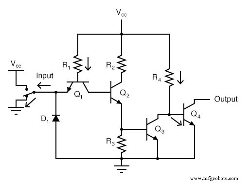
Totem‑Pole Output Variant
The totem‑pole version incorporates complementary NPN/PNP pairs for higher drive strength, but the logical operation remains identical to the open‑collector design.
Key Takeaways
- A pair of inverters in series functions as a buffer, amplifying a weak signal without inverting it.
- Buffer gates are represented by a triangle symbol with no inverter bubble.
- Buffers may employ open‑collector or totem‑pole outputs, each suited to different load‑driving requirements.
Related Worksheet
Industrial Technology
- Understanding the NOT Gate (Inverter) in TTL Circuits
- Understanding Multiple-Input Logic Gates: Functions, Truth Tables, and Practical Applications
- Special-Output Logic Gates: Complementary, Tristate, and Bilateral Switches
- Gated SR Latch: Enhancing Logic Control with an Enable Input
- Mastering the D Latch: A Clean 1‑Bit Memory Circuit
- Understanding the J‑K Flip‑Flop: Design, Logic, and Applications
- Input & Output Coupling Techniques for Amplifiers: Capacitive, Direct, and Transformer Methods
- Silicon‑Controlled Rectifiers (SCRs): Design, Operation, and Practical Applications
- Mastering D Latches: Design, Operation, and Key Differences
- Digital Buffers Explained: A Comprehensive Guide to Signal Isolation & Strength