


Understanding the J‑K Flip‑Flop: Design, Logic, and Applications
The J‑K flip‑flop is a refined bistable multivibrator that resolves the classic S‑R latch’s invalid state. By integrating feedback into the set (S) and reset (R) inputs, it guarantees a valid output for every input combination.
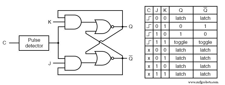
In the diagram below, notice how the traditional 2‑input AND gates have been upgraded to 3‑input AND gates. The third input feeds back from the Q and ¬Q outputs, ensuring that the J and K signals can never activate simultaneously.
The J and K Inputs
Formerly known as S and R, the inputs are now labeled J and K. The 3‑input AND gates use the feedback from Q and ¬Q to selectively inhibit one of the inputs depending on the current state:
- If the circuit is in the set state (Q=1, ¬Q=0), the J input is blocked by the 0 on ¬Q.
- If the circuit is in the reset state (Q=0, ¬Q=1), the K input is blocked by the 0 on Q.
When both J and K are high, the feedback causes a “toggle” behavior on the next clock edge: the flip‑flop flips from set to reset or vice versa.
Logical Sequence of the J‑K Flip‑Flop
Below is the ladder‑logic equivalent that illustrates this behavior step by step.
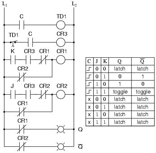
Because the invalid state is removed, the device becomes fully bistable and can be used in reliable sequential circuits. However, without edge‑triggering, holding J=K=1 would turn the circuit into an astable oscillator. Therefore, J‑K flip‑flops are always edge‑triggered—either on the positive or negative edge of the clock.
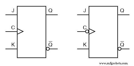
The Block Symbol for J‑K Flip‑Flops
The block diagram is concise and resembles other flip‑flop symbols. J‑K flip‑flops are available in both positive‑edge and negative‑edge triggered versions.
Review
- A J‑K flip‑flop is an S‑R flip‑flop enhanced with feedback that eliminates the invalid condition by ensuring the two inputs never drive the multivibrator simultaneously.
- When J and K are both high and the clock pulses, the outputs toggle, switching from set to reset or the reverse.
Related Worksheets
- J‑K Flip Flops Worksheet
Industrial Technology
- Building a NAND‑Based Set‑Reset Flip‑Flop Circuit
- The 555 Integrated Circuit: A Timeless Benchmark in Analog Design
- The Quadratic Formula: A Reliable Tool for Solving Second‑Degree Equations
- Understanding the Buffer Gate: Amplification and Signal Integrity in Digital Circuits
- Gated SR Latch: Enhancing Logic Control with an Enable Input
- Mastering the D Latch: A Clean 1‑Bit Memory Circuit
- Asynchronous Flip‑Flop Inputs: Preset and Clear Functionality
- Common‑Base Transistor Amplifiers: Design, Analysis, and Applications
- 74LS47 IC Explained: BCD to 7-Segment Decoder Details
- The 74LS74 Dual Flip-Flop: Complete Reference and Pinout