


Building a NAND‑Based Set‑Reset Flip‑Flop Circuit
PARTS AND MATERIALS
- 4011 quad NAND gate (Radio Shack catalog # 276-2411)
- 4001 quad NOR gate (Radio Shack catalog # 276-2401)
- Eight‑position DIP switch (Radio Shack catalog # 275-1301)
- Ten‑segment bar graph LED (Radio Shack catalog # 276-081)
- One 6 V battery
- Three 10 kΩ resistors
- Two 470 Ω resistors
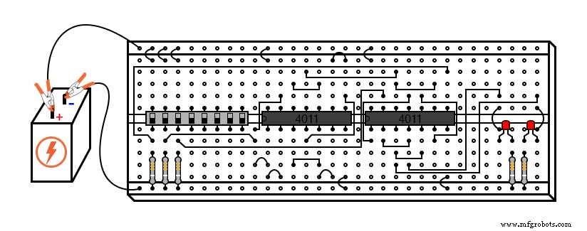
Caution! The 4011 IC is CMOS and therefore highly sensitive to static discharge. While the parts list calls for a ten‑segment LED bar graph, the illustration shows two individual LEDs because of limited breadboard space. If you have enough room, feel free to install the bar graph as originally intended.
CROSS‑REFERENCES
- Lessons In Electric Circuits, Volume 4, Chapter 3: “Logic Gates”
- Lessons In Electric Circuits, Volume 4, Chapter 10: “Multivibrators”
LEARNING OBJECTIVES
- Distinguish between a gated latch and a flip‑flop
- Construct a pulse‑detector circuit that enables edge‑triggered operation
- Understand how mechanical switch bounce can disturb digital logic and learn mitigation strategies
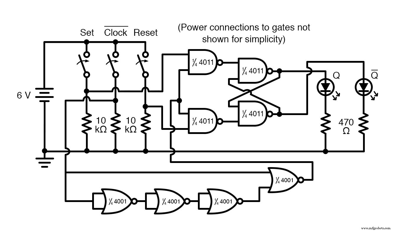
SCHEMATIC DIAGRAM
ILLUSTRATION
INSTRUCTIONS
The core difference between a gated (or enabled) latch and a flip‑flop is the trigger mechanism: a flip‑flop reacts only to a clock edge, whereas a latch follows a sustained enable signal. Converting an enabled latch into a flip‑flop simply requires adding a pulse‑detector that converts a clock edge into a brief high enable pulse.
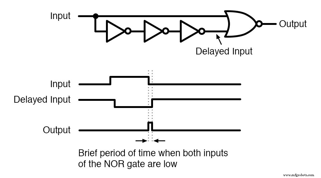
The pulse‑detector uses a single NOR gate and three inverters. By paralleling the NOR inputs, we deliberately slow the propagation to generate a narrow pulse at every falling clock edge.
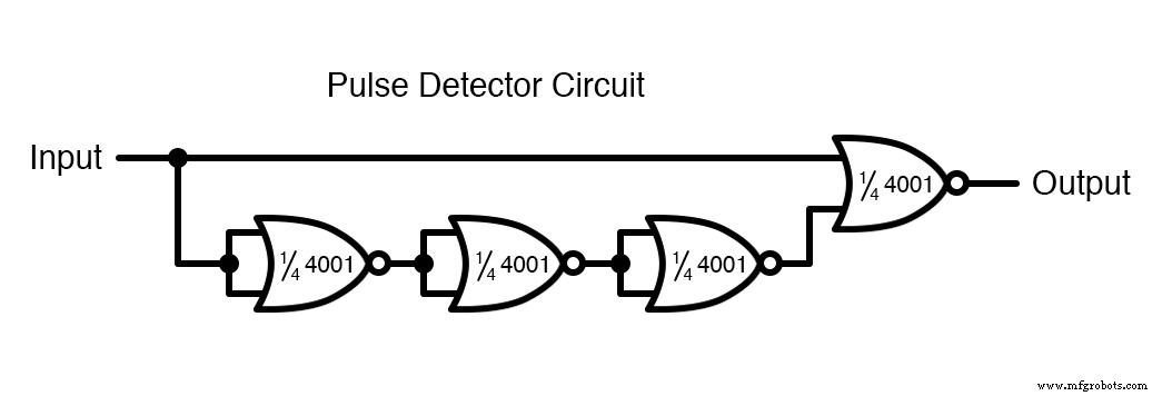
Normally, a NOR gate is wired as an inverter by tying one input to ground and feeding the other with the signal, which minimizes capacitance and maximizes speed. In this circuit we intentionally parallel the inputs to create a sluggish inverter, ensuring the pulse remains long enough to trigger the latch.
This design produces a high output pulse on every falling edge of the clock. Consequently, the SR latch responds to Set and Reset only when the middle switch moves from “on” to “off.” In practice, however, you may observe responses on both transitions because of contact bounce.
Mechanical switches tend to bounce—rapidly opening and closing—when first actuated. This creates multiple low‑high‑low transitions that can inadvertently trigger the pulse‑detector twice, causing the latch to react to both clock edges. Understanding and mitigating contact bounce is essential for reliable digital logic.
RELATED WORKSHEET
- Flip‑Flop Circuits Worksheet
Industrial Technology
- Circuit With a Switch: A Practical Guide to Basic Electrical Circuits
- Commutating Diode Experiment: Suppressing Inductive Kickback with a Neon Lamp
- NOR Gate SR Latch: Building and Understanding Digital Memory
- Building an Enabled NAND‑Gate SR Latch: Parts, Design, and Operation
- Understanding the Buffer Gate: Amplification and Signal Integrity in Digital Circuits
- Understanding Multiple-Input Logic Gates: Functions, Truth Tables, and Practical Applications
- Gated SR Latch: Enhancing Logic Control with an Enable Input
- Understanding the J‑K Flip‑Flop: Design, Logic, and Applications
- Step-by-Step Guide to Wiring a GFCI Combo Switch and Outlet: Diagrams & Installation Tips
- Professional Wiring Guide for Combo Switch/Outlet Devices – Diagrams & Installation Tips