


Edge‑Triggered Latches: From SR/D Latches to Flip‑Flops
In earlier sections we examined S‑R and D latches that respond to data inputs only when an enable (E) signal is active. For many digital designs, it is advantageous to confine the latch’s responsiveness to a very brief interval rather than to the entire duration that the enable line remains high.
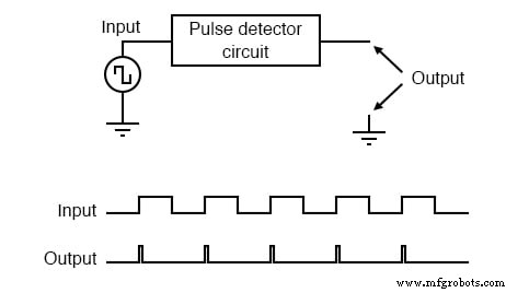
Edge triggering achieves this by allowing the data inputs to influence the latch only during the instant the enable signal transitions from one level to another. This brief window is generated by a pulse detector that produces a short pulse whenever the enable line changes state.
Below we compare timing diagrams for a conventional D latch and an edge‑triggered D latch:
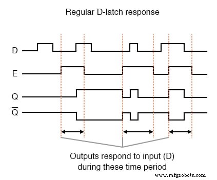
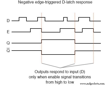
In the first diagram, the output follows input D for as long as the enable (E) signal stays high. Once E returns low, the circuit holds its last state. In the second diagram, the output changes only during the brief instant that E transitions from low to high – this is positive edge triggering.
Negative edge triggering behaves similarly but reacts to the falling edge (high‑to‑low) of the enable signal:
When a latch is driven by a pulse detector on the edge of a clock signal, we refer to it as a flip‑flop rather than a latch. Consequently, an edge‑triggered SR latch becomes an SR flip‑flop, and an edge‑triggered D latch becomes a D flip‑flop. The enable input is renamed the clock (C), and the data inputs (S, R, or D) are called synchronous because they affect the output only at the instant of the clock edge.
How can we implement such edge triggering? Converting a regular SR latch into a gated latch is straightforward with a few AND gates, but generating a pulse that marks only the rising or falling edge of a digital signal requires a dedicated pulse detector. This detector is effectively a monostable multivibrator that produces a short pulse whenever the input toggles.
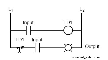
The pulse width is determined by the components inside the detector. In ladder logic, a time‑delay relay with a very short delay accomplishes this:
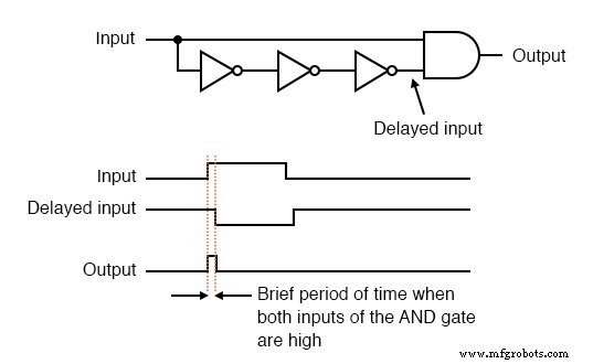
In semiconductor logic, we exploit the propagation delay inherent in logic gates. The input signal is split; one path passes through a gate or series of gates to delay it slightly. The original and delayed signals then feed a two‑input gate that produces a high output only while the delayed signal lags behind the original’s rising edge. An example circuit that generates a pulse on a low‑to‑high transition is shown below:
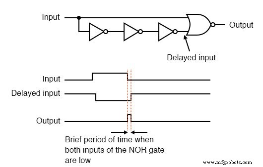
To detect a falling edge, simply replace the final AND gate with a NOR gate:
With a pulse detector in place, we can convert a latch into a flip‑flop. For instance, an SR flip‑flop is obtained by gating the SR latch’s enable line with the pulse detector:
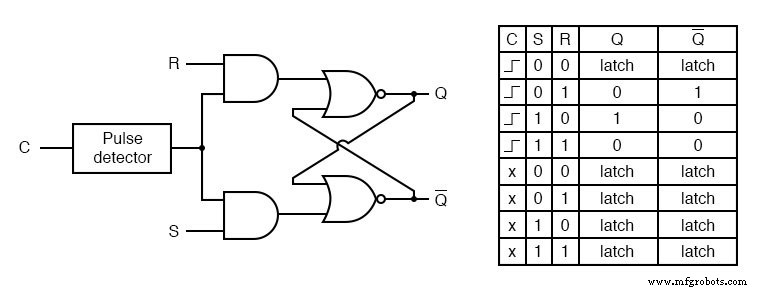
The circuit is responsive to S and R only when the clock (C) transitions from low to high; otherwise, it remains latched. A ladder‑logic representation of the same SR flip‑flop is:
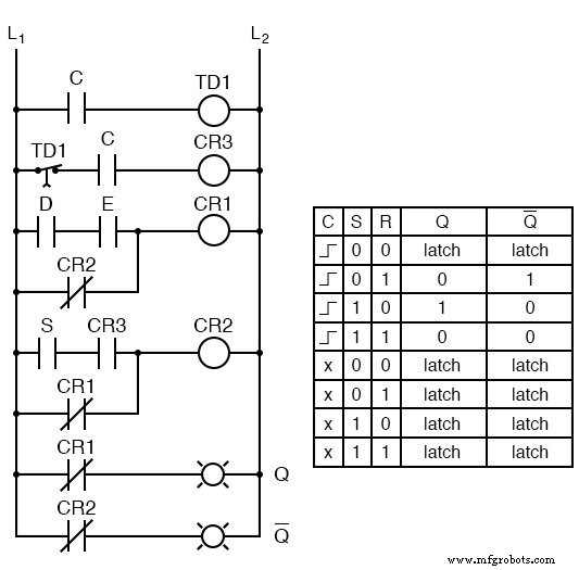
In the ladder diagram, contact CR3 replaces the original enable contact and closes only during the brief window when both C and the time‑delay contact TR1 are closed. Whether implemented with gates or relays, the S and R inputs have no effect unless C is transitioning from 0 to 1.
It is important to note that the SR flip‑flop’s invalid state exists only for the short period during which the pulse detector allows the latch to be enabled. After that window closes, the outputs lock into either the set or reset state. This brief race condition—each latch gate competing to assert its output first—ensures that the flip‑flop settles into a valid, mutually exclusive state.
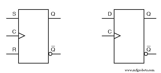
The block symbols for flip‑flops differ slightly from those of latches. The triangle next to the clock input indicates an edge‑triggered device. Positive‑edge flip‑flops are shown with a plain triangle, while negative‑edge devices have a bubble on the clock line:
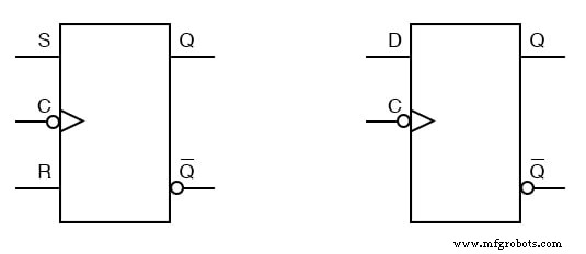
Both diagrams illustrate flip‑flops that clock on the falling edge (high‑to‑low transition) of the clock signal.
REVIEW
- A flip‑flop is a latch equipped with a pulse detector that allows it to respond only to a brief rising or falling edge of the clock.
- Pulse detectors can be implemented with time‑delay relays in ladder logic or with semiconductor gates that use propagation delay.
RELATED WORKSHEETS
- Flip Flops Worksheet
Industrial Technology
- Circuit With a Switch: A Practical Guide to Basic Electrical Circuits
- Voltage Follower Amplifier: Design, Build, and Measurement Guide
- Mastering AC Circuit Equations: Impedance, Reactance & Resonance
- Getting Started with SPICE: A Text‑Based Circuit Simulation Tool
- Mastering SPICE Netlist Syntax: Component Naming, Passive & Active Elements, and Source Definitions
- Demultiplexers Explained: How They Route Signals in Digital Circuits
- Understanding TRIACs: Bidirectional Power Control in AC Applications
- Understanding Electrical Resistance and Circuit Safety
- Understanding Fuses: Types, Ratings, and Safe Installation
- Analyzing Complex RC Circuits Using Thevenin’s Theorem