


Mastering the D Latch: A Clean 1‑Bit Memory Circuit
In a gated S‑R latch, the enable pin allows the Q and Q̅ outputs to remain latched regardless of the S or R signals. By removing one of those inputs, we obtain a multivibrator latch that eliminates any illegal state.
Such a circuit is called a D latch, and its internal logic looks like this:
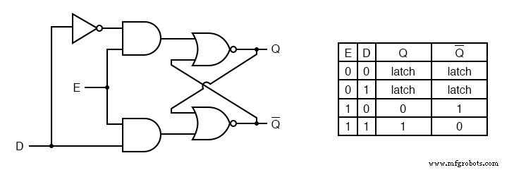
Here, the original R input is replaced by the inverse of the former S input, and the S line is now called D. When the enable (E) is low, the latch ignores changes on D and holds its last value. With E high, the output Q directly tracks D.
Because the R input is eliminated, the D latch never enters an invalid state; Q and Q̅ are always complementary.
If the above diagram is confusing at all, the next diagram should make the concept simpler:
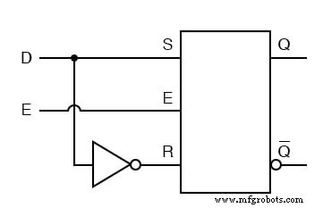
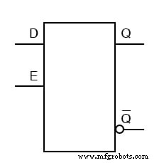
Like both the S‑R and gated S‑R latches, the D latch circuit may be found as its own prepackaged circuit, complete with a standard symbol:
The D latch is nothing more than a gated S‑R latch with an inverter added to make R the complement (inverse) of S.
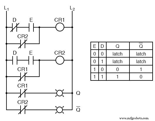
Let’s explore the ladder logic equivalent of a D latch, modified from the basic ladder diagram of an S‑R latch:
The D latch functions as a 1‑bit memory element. To write a value, set enable high and drive D to the desired logic level. When enable is later cleared, the latch retains that value, presenting it on Q while Q̅ outputs the complement.
Key Takeaways:
- The D latch behaves like an S‑R latch but with a single data input. When enable is asserted, the D signal directly sets or resets the latch; with enable deasserted, the output remains unchanged.
- It serves as a 1‑bit RAM cell, holding a high or low value when disabled, and accepting new data on D when enabled.
Related Worksheets:
- Latch Circuits - D Latch Worksheet
Industrial Technology
- The 555 Integrated Circuit: A Timeless Benchmark in Analog Design
- The Quadratic Formula: A Reliable Tool for Solving Second‑Degree Equations
- Understanding the Buffer Gate: Amplification and Signal Integrity in Digital Circuits
- The S‑R Latch: Fundamentals, Race Conditions, and Practical Applications
- Gated SR Latch: Enhancing Logic Control with an Enable Input
- Understanding the J‑K Flip‑Flop: Design, Logic, and Applications
- Common‑Base Transistor Amplifiers: Design, Analysis, and Applications
- DIAC: The Bidirectional Trigger for AC Thyristors
- Mastering D Latches: Design, Operation, and Key Differences
- 74LS47 IC Explained: BCD to 7-Segment Decoder Details