


Common‑Base Transistor Amplifiers: Design, Analysis, and Applications
The common‑base amplifier is the most uncommon of the three basic transistor configurations, largely because its operating characteristics differ markedly from the common‑emitter and common‑collector circuits. This section examines its structure, key performance metrics, and typical use‑cases.
Why the Name “Common‑Base”?
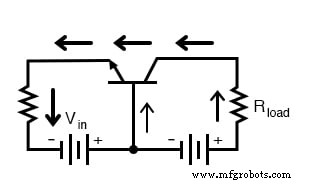
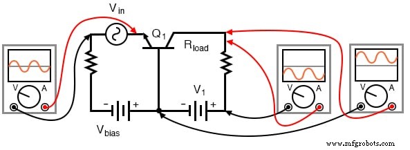
In this topology the signal source and the load share the transistor’s base terminal as a common node (aside from the power supply). The input is applied between emitter and base, while the output is taken between collector and base, as shown in the diagram below.
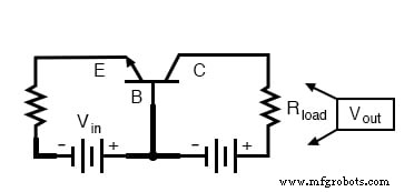
Because the emitter current must flow through the input source, the input signal must carry the full emitter current—typically the largest current in the device. Consequently, the input current can be considerably larger than the output current.
Current Attenuation and Alpha
Since the emitter current dominates, the current gain (output current / input current) is always less than one. This contrasts with the common‑emitter and common‑collector stages, where β (beta) is the key gain parameter. For the common‑base stage the relevant parameter is α (alpha), the ratio of collector to emitter current. By definition, 0 < α < 1, which explains the inherent current attenuation.
Voltage Gain Characteristics
Although the common‑base stage cannot amplify current, it can provide a substantial voltage gain. A SPICE simulation of the circuit below confirms this behavior:
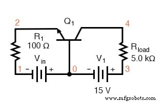
common-base amplifier vin 0 1 r1 1 2 100 q1 4 0 2 mod1 v1 3 0 dc 15 rload 3 4 5k .model mod1 npn .dc vin 0.6 1.2 .02 .plot dc v(3,4) .end
The DC transfer curve shows the output voltage rising from near zero (cut‑off) to 15.75 V as the input voltage sweeps from 0.6 V to 1.2 V. The voltage gain, defined as the ratio of the output span (15.75 V) to the input span (0.42 V), is 37.5 (≈ 31.5 dB). The output can exceed the supply voltage due to the series‑aiding effect of the input source.
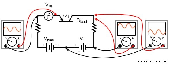
A similar trend appears in the AC simulation, where the input and output are in phase, confirming that the common‑base stage is non‑inverting.
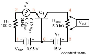
common-base amplifier vin 5 2 sin (0 0.12 2000 0 0) vbias 0 1 dc 0.95 r1 2 1 100 q1 4 0 5 mod1 v1 3 0 dc 15 rload 3 4 5k .model mod1 npn .tran 0.02m 0.78m .plot tran v(5,2) v(4) .end
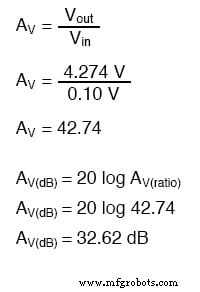
At 2 kHz the AC analysis yields a voltage gain of 42.74 (≈ 32.6 dB). The phase diagram below illustrates the signal relationships and DC offsets for both NPN and PNP devices.
Predicting Voltage Gain
Unlike the other two configurations, the voltage gain of a common‑base amplifier depends heavily on the DC bias point. The emitter‑base junction’s dynamic resistance changes with emitter current, making analytical predictions challenging. Computer simulations can capture this behavior effectively. For example, varying the bias voltage while keeping the AC amplitude constant alters the gain, as shown in the table below.
common-base amp vbias=0.85V vin 5 2 sin (0 0.12 2000 0 0) vbias 0 1 dc 0.85 r1 2 1 100 q1 4 0 5 mod1 v1 3 0 dc 15 rload 3 4 5k .model mod1 npn *.tran 0.02m 0.78m .tf v(4) vin .end
The SPICE output for bias values from 0.85 V to 1.00 V shows a clear trend: the transfer function (voltage gain) rises from 37.6 to 44.0 as the bias increases. The corresponding input impedance decreases slightly, while the output impedance remains fixed at 5 kΩ.
In all cases the current gain (I(v1)/Iin) hovers near 0.99, consistent with α ≈ β/(β+1) for β ≈ 100.
Practical Applications
Due to its high voltage gain, low input impedance, and reduced susceptibility to parasitic capacitances, the common‑base topology is favored in radio‑frequency (RF) amplifiers and high‑speed signal paths. Its grounded base offers excellent shielding of the emitter input from collector noise, enhancing stability at high frequencies. Classic examples include Class C RF power amplifiers and Class A small‑signal high‑gain stages.
Key Take‑aways
- The base terminal is common to both input and output, which defines the name.
- Current gain is always < 1; voltage gain can be very high and depends on bias.
- Alpha (α) governs the current ratio; it remains below unity for all transistors.
Further Reading
Industrial Technology
- Understanding the Common-Emitter Amplifier: Switching, Amplification, and Biasing Techniques
- Common‑Collector Amplifier: Emitter‑Follower Fundamentals & Applications
- Cascode Amplifier: Combining Common‑Emitter and Common‑Base for Wide Bandwidth and High Input Impedance
- Common-Source JFET Amplifier: Design, Analysis, and Practical Worksheet
- Common-Drain JFET Amplifier: Fundamentals, Applications & Worksheet
- Common‑Source Amplifier (IGFET): Design, Biasing, and Performance
- Common‑Drain Amplifier (IGFET): Design, Function, and Applications
- Common‑Gate IGFET Amplifier: Theory, Design, and Practical Applications
- The Operational Amplifier: Foundations, Features, and Key Applications
- Understanding and Designing an Instrumentation Amplifier