


Understanding the Common-Emitter Amplifier: Switching, Amplification, and Biasing Techniques
The common‑emitter configuration is a foundational transistor circuit that serves both as a robust switch and as an effective amplifier for analog signals. By operating between its saturation and cutoff limits, a transistor can precisely control collector current, enabling linear amplification of input currents or voltages.
Transistor as a Simple Switch
In a classic NPN switch, the emitter serves as a common node for both the signal source and the load. The schematic below illustrates the transistor’s two extreme operating modes:
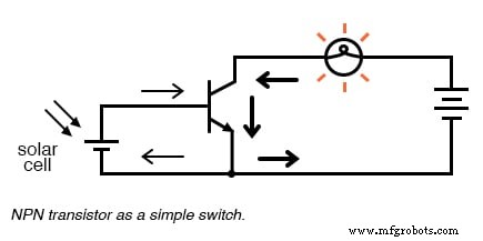
When a solar cell generates a small current, the transistor can saturate and drive a lamp. The lamp’s brightness is directly proportional to the light intensity falling on the cell.
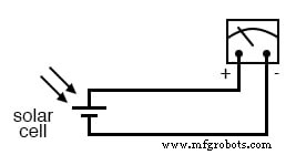
Using the Solar Cell as a Light‑Intensity Meter
Directly wiring a meter movement to a solar cell works for moderate light levels but limits sensitivity because the cell must supply all the meter’s power. Amplification is therefore required for low‑intensity measurements.
Amplifying Solar‑Cell Current
Inserting a common‑emitter transistor boosts the current seen by the meter by a factor of β (often 100), allowing far greater deflection for the same incident light. The additional power needed to move the meter comes from an external battery; the transistor simply regulates that current.
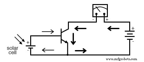
Because the meter deflection depends only on the solar‑cell current, the reading remains accurate regardless of battery voltage variations, provided the battery can deliver the required current.
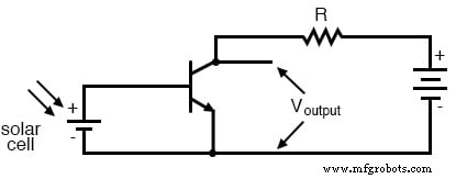
Voltage Output from a Load Resistor
Replacing the meter with a resistor and measuring the collector‑emitter voltage produces an inverted voltage output that varies linearly with the input current until saturation. In saturation, the collector‑emitter voltage never drops to zero due to the transistor’s junctions.
Simulation: Collector Voltage vs. Base Current
SPICE simulations confirm the expected behavior: the output voltage decreases from the supply voltage to a few tenths of a volt as the transistor moves from cutoff to saturation.
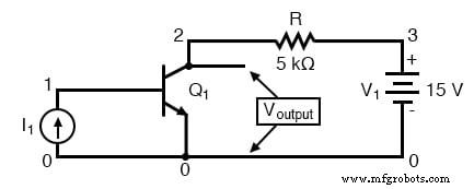
*common-emitter amplifier
i1 0 1 dc q1 2 1 0 mod1 r 3 2 5000
v1 3 0 dc 15
.model mod1 npn
.dc i1 0 50u 2u
.plot dc v(2,0)
.end
Output voltage traces show a perfectly linear drop from 15 V to about 1 V until saturation, followed by a sharp decline that asymptotically approaches zero.
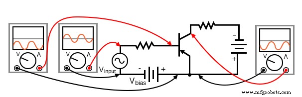
From DC to AC: Amplifying Audio Signals
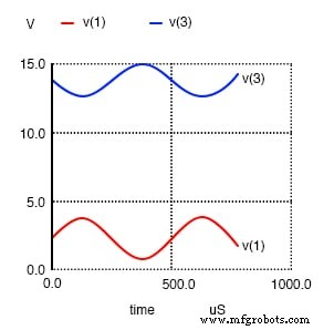
Common‑emitter amplifiers are also used to boost audio signals. A microphone’s AC output can drive a transistor if the base‑emitter junction remains forward‑biased throughout the waveform, which requires a DC bias added in series with the audio source.
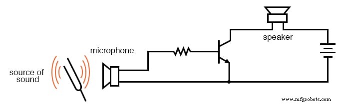
Without bias, the transistor remains in cutoff for half the cycle, producing a clipped output and audible distortion.
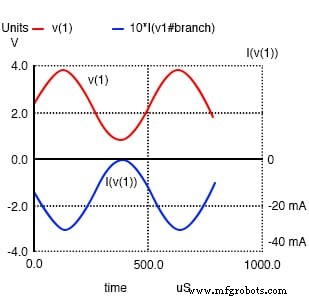
common-emitter amplifier
vinput 1 5 sin (0 1.5 2000 0 0)
vbias 5 0 dc 2.3
r1 1 2 1k
q1 3 2 0 mod1
rspkr 3 4 8
v1 4 0 dc 15
.model mod1 npn
.tran 0.02m 0.78m
.plot tran v(1,0) i(v1)
.end
With the bias voltage, the transistor stays active throughout the cycle, faithfully reproducing the audio waveform at the speaker and avoiding distortion.
Biasing Fundamentals
Biasing is essential for AC amplification with bipolar transistors because these devices are inherently current‑controlled and allow current flow only in one direction. A DC bias ensures continuous forward bias of the base‑emitter junction.
Gain Calculations
The current gain equals the transistor’s β (≈100 in our simulations), giving a 40 dB current gain. Voltage gain, however, depends on the ratio of load resistance (Rout) to input resistance (Rin), and can be expressed as:
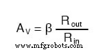
Increasing the load resistance from 8 Ω to 30 Ω raised the output voltage from roughly 1 V to 4.4 V, yielding a voltage gain of 2.95 (≈9.4 dB) as verified by SPICE AC analysis.
common-emitter amplifier
vinput 1 5 sin (0 1.5 2000 0 0)
vbias 5 0 dc 2.3
r1 1 2 1k
q1 3 2 0 mod1
rspkr 3 4 30
v1 4 0 dc 15
.model mod1 npn
.tran 0.02m 0.78m
.plot tran v(1,0) v(3)
.end
PNP Equivalent
PNP transistors can be used in the same common‑emitter configuration, yielding identical gain and inversion characteristics; only the supply polarity reverses.
Key Takeaways
- The common‑emitter amplifier shares the emitter node between input and output.
- Biasing with a DC offset is mandatory for AC signal amplification to keep the transistor in its active region.
- Collector‑emitter voltage is 180° out of phase with the base‑emitter input—hence, an inverting amplifier.
- Current gain ≈ β; voltage gain depends on Rout/Rin.
Industrial Technology
- Common‑Emitter Amplifier: Design, Measurement, and Feedback Techniques
- Understanding the NOT Gate (Inverter) in TTL Circuits
- Common‑Collector Amplifier: Emitter‑Follower Fundamentals & Applications
- Common‑Base Transistor Amplifiers: Design, Analysis, and Applications
- Cascode Amplifier: Combining Common‑Emitter and Common‑Base for Wide Bandwidth and High Input Impedance
- Common‑Source Amplifier (IGFET): Design, Biasing, and Performance
- Common‑Drain Amplifier (IGFET): Design, Function, and Applications
- Common‑Gate IGFET Amplifier: Theory, Design, and Practical Applications
- DIAC: The Bidirectional Trigger for AC Thyristors
- Understanding and Designing an Instrumentation Amplifier