


Common‑Emitter Amplifier: Design, Measurement, and Feedback Techniques
Parts and Materials
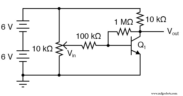
- One NPN transistor (model 2N2222 or 2N3403 recommended; a 15‑unit pack is listed in the Radio Shack catalog #276‑1617)
- Two 6‑V batteries
- One 10 kΩ potentiometer, single‑turn, linear taper (Radio Shack catalog #271‑1715)
- One 1 MΩ resistor
- One 100 kΩ resistor
- One 10 kΩ resistor
- One 1.5 kΩ resistor
Cross‑References
Lessons In Electric Circuits, Volume 3, Chapter 4: Bipolar Junction Transistors
Learning Objectives
- Design a simple common‑emitter amplifier circuit
- Measure amplifier voltage gain
- Distinguish between inverting and non‑inverting amplifiers
- Apply negative feedback to improve stability
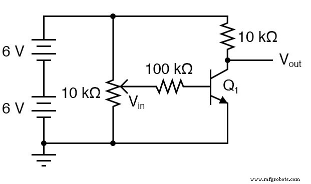
Schematic Diagram
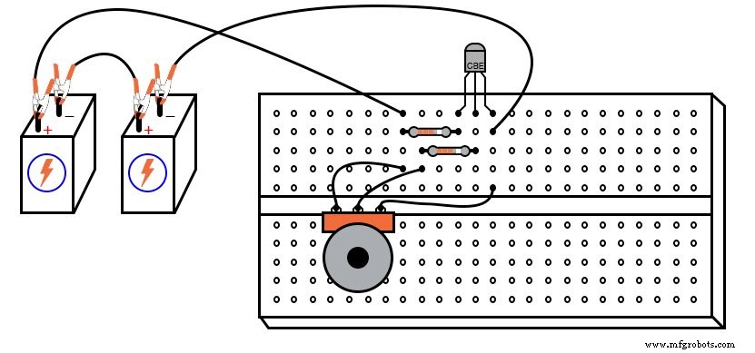
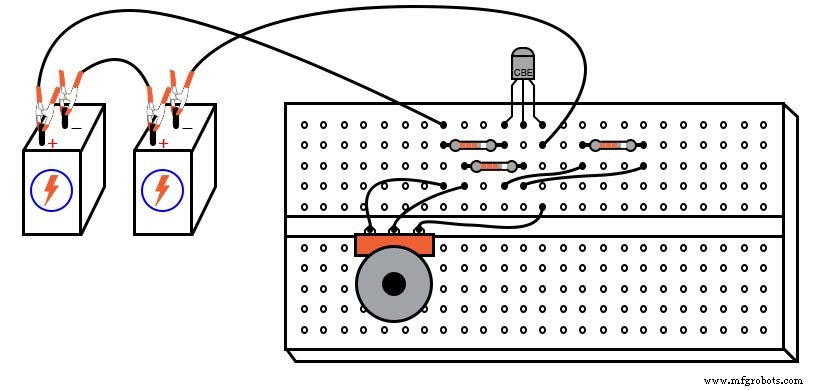
Illustration
Instructions
Build the circuit and measure the output voltage (collector‑to‑ground) and input voltage (potentiometer wiper‑to‑ground) across a range of potentiometer settings. First sweep the potentiometer from its lowest to highest position to identify the full output voltage span. Then pick several intermediate target voltages (e.g., 1 V, 3 V, 5 V, 7 V, 9 V, 11 V) and record the corresponding input voltages.
With at least two data pairs, calculate voltage gain as the ratio of output change to input change. For example, if 1.5 V input yields 7.0 V output and 1.66 V input yields 1.0 V output, the gain is (7.0–1.0)/(1.66–1.5) = 6/0.16 ≈ 37.5.
Two key observations emerge: inversion – increasing input voltage produces a decreasing output voltage, confirming the amplifier is inverting; and a large voltage gain, far exceeding the unity gain of a voltage follower.
Common‑emitter amplifiers are prized for their high gain but are also sensitive to temperature. Test this by heating the transistor (hand or hair dryer) and noting any shift in output voltage at a fixed input. Conversely, cool the transistor with an ice cube and observe the change. Temperature variations alter the base‑emitter junction, modifying base current for a given input and thereby affecting collector current and output voltage.
Negative feedback can mitigate temperature drift. The simplest method adds a resistor between emitter and ground, creating a voltage divider that reduces input sensitivity. See the diagram below for reference.
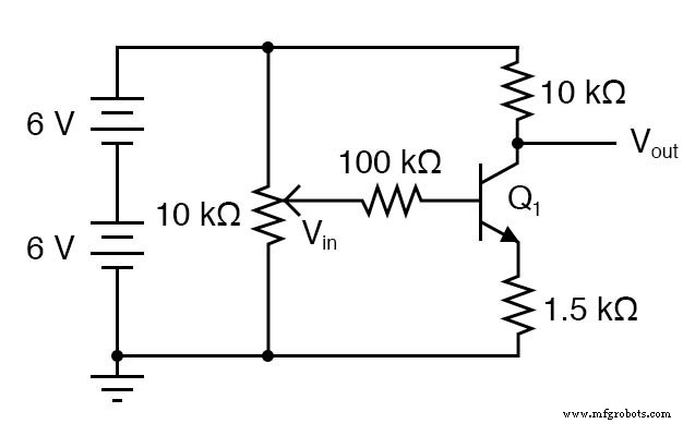
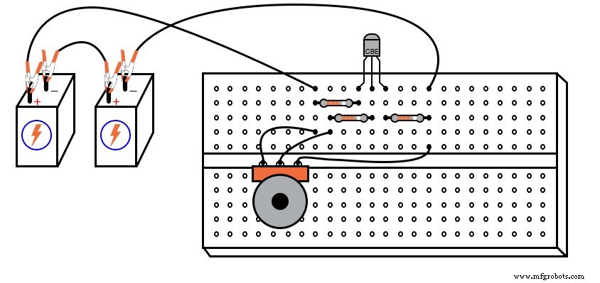
Repeat the voltage measurements with a 1.5 kΩ emitter resistor installed. Re‑calculate the reduced gain and test temperature stability again. Compare the magnitude of output variation with and without the resistor.
An alternative feedback technique couples the output back to the input via a high‑value resistor (e.g., 1 MΩ between collector and base). This also lowers gain while enhancing stability, though the two schemes yield different output ranges. Observe how the full‑sweep voltage limits differ between the two circuits.
Computer Simulation
Schematic with SPICE node numbers:
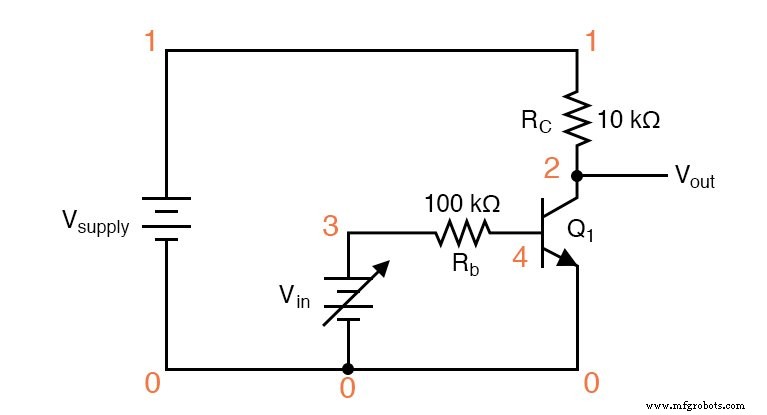
Netlist (create a text file containing the following exactly):
Common‑emitter amplifier vsupply 1 0 dc 12 vin 3 0 rc 1 2 10k rb 3 4 100k q1 2 4 0 mod1 .model mod1 npn bf=200 .dc vin 0 2 0.05 .plot dc v(2,0) v(3,0) .end
This SPICE simulation applies a DC sweep from 0 to 2 V on vin and records the collector‑to‑ground voltage. The output plot shows a step‑like transition when the transistor enters its active region.
Related Worksheet
- Class A BJT Amplifiers Worksheet
Industrial Technology
- Designing a High‑Gain Multi‑Stage Common‑Emitter Amplifier with Negative Feedback
- Designing a High‑Gain Differential Amplifier with NPN Transistors
- Build a High‑Gain Differential Amplifier That Works as an Op‑Amp
- Precision Voltage Follower: Mastering Op‑Amp Feedback for Accurate Signal Tracking
- Non‑Inverting Amplifier: Build, Test, and Master Op‑Amp Gain Control
- Understanding Amplifier Gain: Voltage, Current, and Power
- Common‑Collector Amplifier: Emitter‑Follower Fundamentals & Applications
- Understanding Negative Feedback in Op‑Amps: Voltage Followers and Stability
- Positive Feedback in Op‑Amp Circuits: Hysteresis, Comparators, and Oscillators
- Understanding Voltage Amplifiers: How They Boost Signal Voltage