


Build a High‑Gain Differential Amplifier That Works as an Op‑Amp
Parts and Materials
- Two 6‑volt batteries
- Four NPN transistors—models 2N2222 or 2N3403 (Radio Shack catalog # 276‑1617 provides a convenient pack of fifteen NPN devices)
- Two PNP transistors—models 2N2907 or 2N3906 (Radio Shack catalog # 276‑1604 offers a pack of fifteen PNPs)
- Two 10 kΩ potentiometers, single‑turn, linear taper (Radio Shack catalog # 271‑1715)
- One 270 kΩ resistor
- Three 100 kΩ resistors
- One 10 kΩ resistor
Cross‑References
Lessons In Electric Circuits, Volume 3, chapters 4 “Bipolar Junction Transistors” and 8 “Operational Amplifiers.”
Learning Objectives
- Design a differential amplifier that uses current mirrors.
- Explore how negative feedback shapes the behavior of a high‑gain differential amplifier.
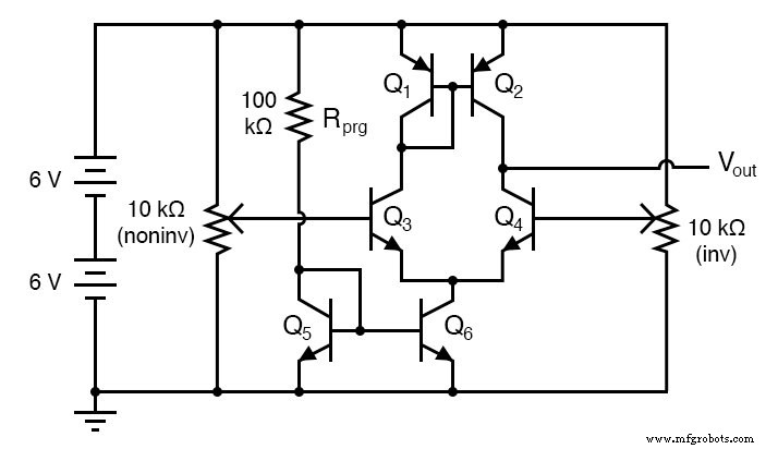
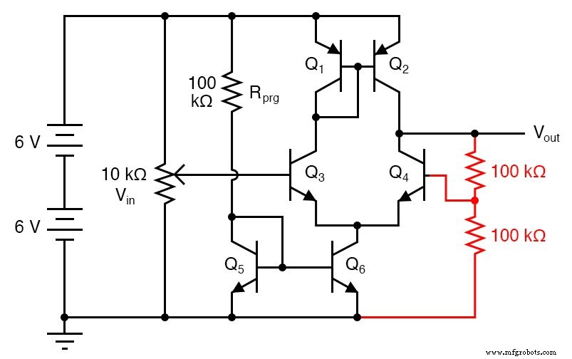
Schematic Diagram
Illustration
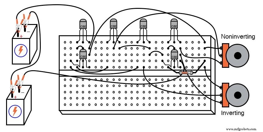
Instructions
This design refines the earlier differential amplifier by replacing voltage‑drop resistors with current‑mirror networks, yielding a higher voltage gain and more predictable performance.
With its increased gain, the circuit can operate as a functional operational amplifier (op‑amp). Op‑amps are the cornerstone of modern analog electronics, so understanding their internal structure is invaluable.
The PNP pair Q1 and Q2 forms a current mirror that keeps the currents through the differential pair Q3 and Q4 balanced. The NPN pair Q5 and Q6 provides a second current mirror that fixes the total differential‑pair current via the programmable resistor R_prg.
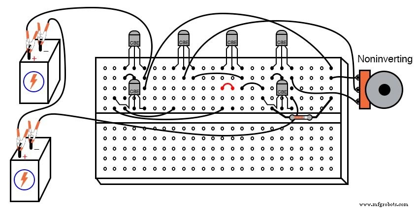
Measure the output voltage (collector of Q4 relative to ground) while varying the two input voltages. Notice that one potentiometer acts as a non‑inverting input, while the other serves as the inverting input.
The output responds most strongly when the two inputs are nearly equal—this is the differential mode. Once that behavior is confirmed, the circuit can be used as a true op‑amp. A common first experiment is the voltage‑follower (buffer) configuration.
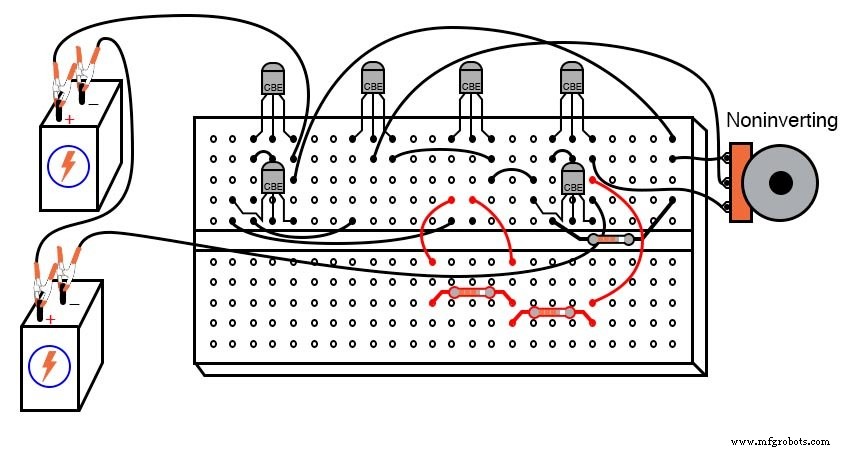
For a voltage follower, connect the output of the amplifier directly to its inverting input—i.e., tie the collector and base of Q4 together and ignore the inverting potentiometer.
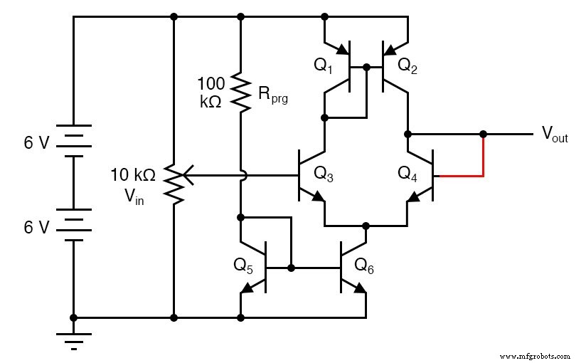
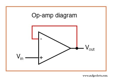
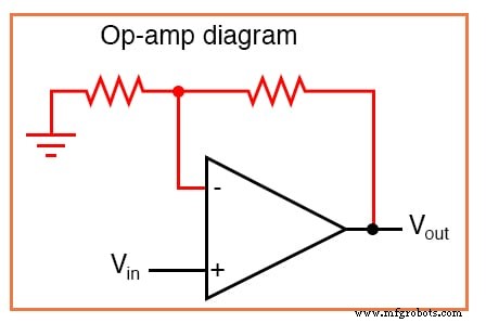
The op‑amp symbol shows the non‑inverting (+) and inverting (−) inputs and the output apex. The red trace represents the feedback loop. In a voltage follower the output should track the input within a few hundredths of a volt.
A more sophisticated arrangement is the non‑inverting amplifier, where two equal resistors in the feedback loop set a gain of exactly two.
During testing you may see small discrepancies between the measured and expected output—usually a few hundredths of a volt. These arise from imperfections in the differential pair and can be reduced by adding extra amplification stages or by fine‑tuning R_prg.
Try different R_prg values ranging from 10 kΩ to 1 MΩ. Avoid resistances below 10 kΩ to prevent thermal runaway in the current‑mirror transistors.
Some commercial op‑amps expose a programmable current‑mirror point, allowing users to adjust the internal bias exactly like R_prg. Most factory‑made op‑amps, however, have this bias fixed by a precisely trimmed resistor.
Industrial Technology
- Simple Analog Averaging Circuit: A Practical Voltage Averager
- Common‑Emitter Amplifier: Design, Measurement, and Feedback Techniques
- Voltage Comparator Circuit – Build and Test with a Dual Op‑Amp
- Precision Voltage Follower: Mastering Op‑Amp Feedback for Accurate Signal Tracking
- Integrating (Single‑Slope) ADCs: Principles, Advantages, and Dual‑Slope Alternatives
- Understanding Negative Feedback in Op‑Amps: Voltage Followers and Stability
- Positive Feedback in Op‑Amp Circuits: Hysteresis, Comparators, and Oscillators
- Practical Considerations for Operational Amplifiers
- Vector Addition and AC Voltage Superposition: A Practical Guide
- Timers & Multi-Vibrators: Types, Functions, and Digital Applications