


Flash ADC (Parallel Analog‑to‑Digital Converter) – Design, Operation, and Applications
Also known as a parallel A/D converter, the flash ADC is the most straightforward ADC architecture. It consists of a series of comparators, each comparing the analog input to a distinct reference voltage. The comparator outputs feed a priority encoder that generates a binary output. The diagram below illustrates a 3‑bit flash ADC:
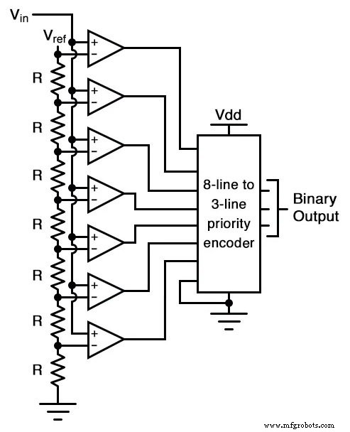
The reference voltage (Vref) is supplied by a precision voltage regulator—though the regulator itself is omitted from the schematic for clarity. As the input voltage rises above successive reference levels, the comparators saturate to a high state in sequence. The priority encoder then produces a binary number corresponding to the highest‑order active comparator, effectively ignoring lower‑order signals.
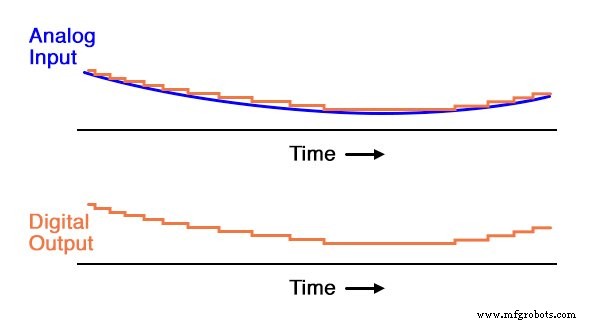
When the ADC operates, its output typically appears as follows:
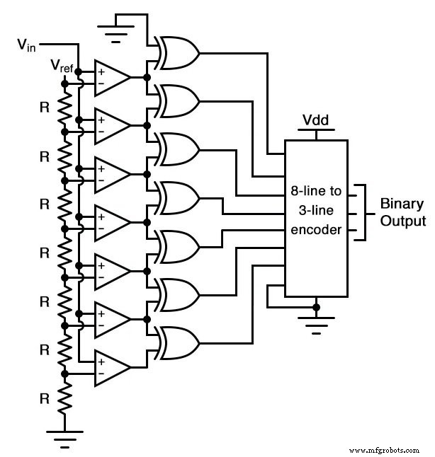
In many practical designs, a full‑featured priority encoder is unnecessary. Because the comparator outputs rise sequentially from the lowest to the highest reference, the highest‑order active input can be selected using a simple network of exclusive‑OR gates, eliminating the need for a complex encoder:
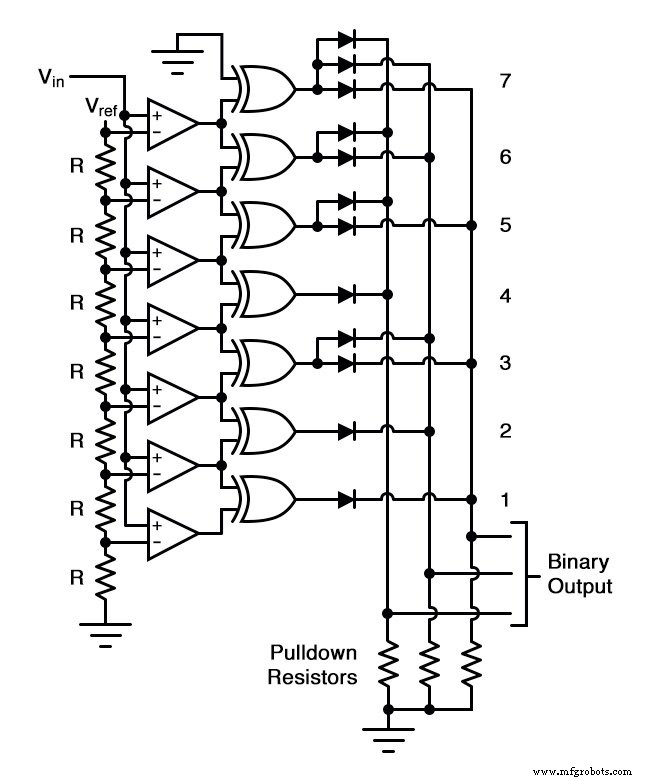
Moreover, the encoder can be realized with a matrix of diodes, underscoring the minimal component count achievable with this topology:
The flash ADC’s simplicity is matched by its speed; it is limited only by the propagation delays of comparators and logic gates. However, the architecture is highly component‑intensive: a 3‑bit converter requires seven comparators, a 4‑bit version needs fifteen, and each additional bit doubles the count. Consequently, an 8‑bit flash ADC would need 255 comparators—an impractical number for most applications.
Despite its component cost, the flash ADC offers unique advantages. With equal‑value resistors in the reference divider, each binary count corresponds to an identical analog increment, yielding a linear response. For specialized applications, adjusting the divider values can create a custom, non‑linear mapping—an ability no other ADC architecture offers without significant redesign.
RELATED WORKSHEET:
- Analog-to-Digital Conversion Worksheet
Industrial Technology
- Exploring Voltage Addition with Series Battery Connections
- Voltage Divider Lab: Design, Measurement, and Kirchhoff’s Voltage Law Verification
- Thermoelectricity: Understanding Thermocouples and the Seebeck Effect
- Potentiometric Voltmeter: Precise Voltage Measurement with Minimal Loading
- Build a Potato Battery: A Step‑by‑Step Guide to DIY Electrochemical Power
- Low‑Voltage AC Power Supply: Phase‑Shift Circuit Components & Best Practices
- Voltage Regulator Experiment with a 12‑Volt Zener Diode
- Integrating (Single‑Slope) ADCs: Principles, Advantages, and Dual‑Slope Alternatives
- Tachogenerators: Precision Speed Measurement for Industrial Motors and Equipment
- Understanding AC Waveforms: Sine Waves, Frequency, and Oscilloscope Basics