


Practical Considerations for Operational Amplifiers
Real operational amplifiers deviate from the ideal model in several ways: input offset, finite common‑mode rejection, input bias currents, temperature drift, and frequency‑dependent gain and phase. Understanding these non‑idealities is essential for designing robust analog circuits. While many errors are negligible in simple applications, they can become critical in precision instrumentation, signal conditioning, or high‑speed systems. In some cases, the effect can be compensated; in others, a higher‑quality, higher‑cost device may be required.
Common‑Mode Gain
In an ideal differential amplifier the output is strictly a function of the voltage difference between its two inputs. When the inputs are shorted together (zero differential voltage) any applied common‑mode voltage, VCM, should not alter the output. The ideal common‑mode voltage gain is therefore zero.
Real op‑amps, however, exhibit a small common‑mode gain. The common‑mode rejection ratio (CMRR) is defined as the ratio of differential to common‑mode gain:

For the classic 741, CMRR averages around 70 dB, equivalent to a ratio of roughly 3,000:1. Because the differential gain is typically orders of magnitude larger, the impact of common‑mode gain is usually minor when negative feedback is employed. Nonetheless, in instrumentation‑type configurations, resistor mismatch can introduce significant common‑mode gain, as demonstrated below.
Below is a SPICE simulation of an instrumentation amplifier with the inputs shorted and a varying common‑mode voltage. In the perfectly balanced circuit the output remains at zero volts across the entire sweep:
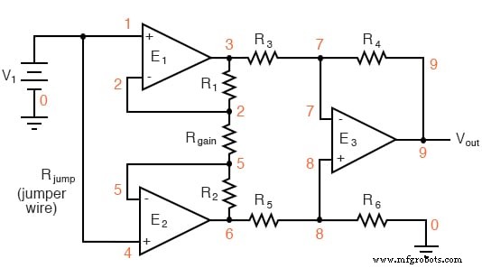
instrumentation amplifier v1 1 0 rin1 1 0 9e12 rjump 1 4 1e-12 rin2 4 0 9e12 e1 3 0 1 2 999k e2 6 0 4 5 999k e3 9 0 8 7 999k rload 9 0 10k r1 2 3 10k rgain 2 5 10k r2 5 6 10k r3 3 7 10k r4 7 9 10k r5 6 8 10k r6 8 0 10k .dc v1 0 10 1 .print dc v(9) .end
v1 v(9) 0.000E+00 0.000E+00 1.000E+00 1.355E-16 2.000E+00 2.710E-16 3.000E+00 0.000E+00 4.000E+00 5.421E-16 5.000E+00 0.000E+00 6.000E+00 0.000E+00 7.000E+00 0.000E+00 8.000E+00 1.084E-15 9.000E+00 -1.084E-15 1.000E+01 0.000E+00
Introducing a small resistor imbalance (e.g., raising R5 from 10 kΩ to 10.5 kΩ) produces a measurable common‑mode gain, as seen in the following output sweep:
v1 v(9) 0.000E+00 0.000E+00 1.000E+00 -2.439E-02 2.000E+00 -4.878E-02 3.000E+00 -7.317E-02 4.000E+00 -9.756E-02 5.000E+00 -1.220E-01 6.000E+00 -1.463E-01 7.000E+00 -1.707E-01 8.000E+00 -1.951E-01 9.000E+00 -2.195E-01 1.000E+01 -2.439E-01
Although the input differential remains zero, the output now varies by ~0.24 V across a 0‑10 V common‑mode sweep, illustrating how resistor mismatch can generate undesirable common‑mode gain. The remedy is straightforward: ensure precise resistor matching and, if possible, include a trim potentiometer on the final op‑amp’s feedback network to null residual common‑mode gain.
Offset Voltage
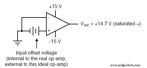
Offset voltage is the voltage that appears at the output when the two inputs are shorted together. Ideally this would be zero; in practice, it is often a few millivolts and can drive the output to saturation, especially in single‑supply designs. Offset is expressed as an equivalent input voltage that would produce the observed output when applied to a perfectly ideal amplifier:
Manufacturers provide offset‑null pins on many op‑amps (e.g., pins 1 and 5 on the 741’s 8‑pin DIP). By connecting a small potentiometer between these pins and the input bias voltage, the user can fine‑tune the offset to near zero. Not all op‑amps expose offset‑null pins; consult the datasheet for the specific part.
Bias Current
Op‑amps have high input impedance, but the bias current—usually a few microamps—is required to operate the internal input stage. In circuits where a single input is connected to a high‑impedance source (e.g., a thermocouple or a pH electrode), the bias current can create a voltage drop across the series resistance, leading to measurement errors.
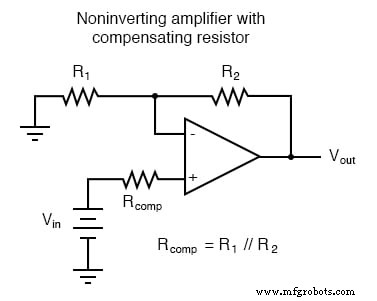
For example, in a voltage‑follower configuration with a 1 MΩ source resistor, a 10 µA bias current produces a 10 mV error. The common technique to mitigate this is to add a resistor of equal value to the other input, thus balancing the bias‑current voltage drops:
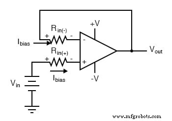
In inverting or non‑inverting amplifiers, the compensating resistor is chosen to match the parallel combination of the two resistors in the feedback network:
Proper grounding of the power supply is also critical. Without a common ground, bias currents have no path to flow, rendering the op‑amp’s input stage ineffective. Always ensure that one terminal of the supply is connected to the circuit ground reference.
Drift
Temperature variations cause the bias current, offset voltage, and other parameters to drift. The extent of drift varies with device technology; JFET or MOSFET input op‑amps generally exhibit lower drift than bipolar designs. Selecting a low‑drift part and, where high accuracy is required, maintaining a stable temperature environment (e.g., with a temperature‑controlled enclosure) are the most effective countermeasures.
Frequency Response
High differential gain makes op‑amps prone to feedback oscillation. A simple voltage‑follower built with a 3130 can oscillate unless a compensation capacitor is added between the two special “compensation” pins. Even when a capacitor is internal (as in the 741), the AC gain falls off with frequency, limiting the usable bandwidth.
Manufacturers publish frequency‑response curves (gain vs. frequency). Designers must reference these when specifying the closed‑loop bandwidth to avoid performance degradation or instability.
Input‑to‑Output Phase Shift
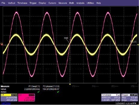
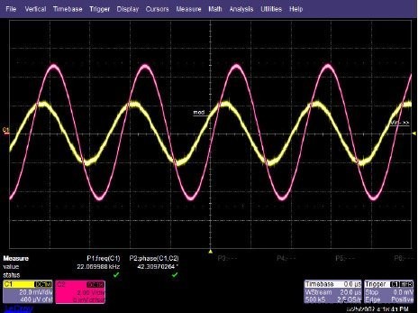
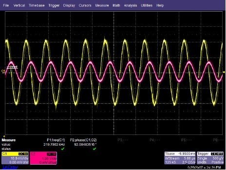
To illustrate phase shift, we measured the OPA227 in a non‑inverting configuration with a 34× gain (~50 dB). The open‑loop gain intersects the 50 dB closed‑loop line at about 22 kHz, establishing a dominant pole. Consequently, the closed‑loop phase shifts as follows:
- ~0° at 2.2 kHz (one decade below the pole)
- ~45° at 22 kHz (at the pole)
- ~90° at 220 kHz (one decade above the pole)
Oscilloscope captures confirm these predictions: no phase shift at 2.2 kHz, ~45° at 22 kHz, and ~90° at 220 kHz.
Related Worksheets
- Summer and Subtractor Op‑Amp Circuits Worksheet
- Inverting and Non‑inverting Op‑Amp Voltage Amplifier Circuits Worksheet
Industrial Technology
- Build a High‑Gain Differential Amplifier That Works as an Op‑Amp
- Voltage Comparator Circuit – Build and Test with a Dual Op‑Amp
- Key ADC Design Factors: Resolution, Sampling, and Practical Performance
- Determinism and Fault Tolerance: Essential Design Principles for Industrial Control Networks
- Voltage and Current in a Practical Circuit: Understanding Their Relationship
- Practical Battery Bank Design: Series vs Parallel, Protection, and Charging Best Practices
- Practical Considerations for Selecting and Using Capacitors
- Practical Considerations for Selecting and Using Inductors
- Practical Considerations in Transformer Design: Power, Losses, and Performance
- 10 Essential Tips for Designing Low‑Noise Amplifiers