


Designing and Verifying a Basic NAND Gate Circuit with the 4011 IC
Parts and Materials
- 4011 quad NAND gate (Radio Shack catalog # 276‑2411)
- Eight‑position DIP switch (Radio Shack catalog # 275‑1301)
- Ten‑segment bar graph LED (Radio Shack catalog # 276‑081)
- One 6‑volt battery
- Two 10 kΩ resistors
- Three 470 Ω resistors
Caution! The 4011 IC is CMOS and is highly sensitive to static discharge. Handle with anti‑static precautions.
Further Reading
Lessons In Electric Circuits, Volume 4, chapter 3: “Logic Gates.”
Learning Objectives
- Understand the role of a pulldown resistor.
- Determine a gate’s truth table through experiment.
- Learn how to interconnect logic gates.
- Design various logical functions using NAND gates.
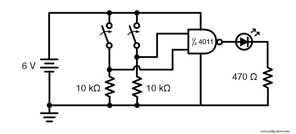
Basic Gate Function Schematic Diagram
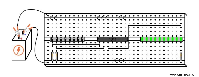
Basic Gate Function Illustration
Experiment Instructions
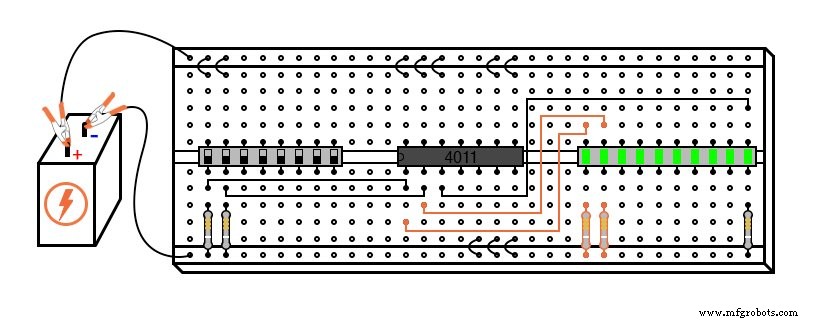
Begin by wiring a single NAND gate to two input switches and one LED, as shown in the schematic. The eight‑position switch and ten‑segment LED may appear excessive at first, but they enable easy expansion and keep the layout tidy.
Always keep a datasheet for the 4011 handy. Reading the pin‑out diagram is essential for correct connections. Below is a simplified pin‑out reference derived from the official datasheet:
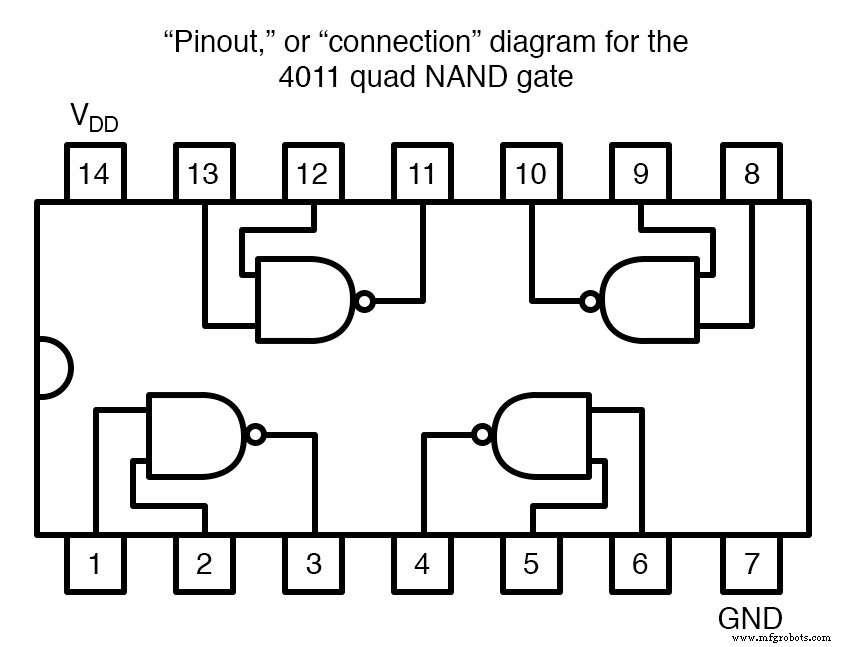
In the breadboard illustration, we use the lower‑left NAND gate: pins 1 and 2 are the inputs, and pin 3 is the output. Pins 14 and 7 supply VDD (positive voltage) and GND (ground). Some datasheets label the negative rail as VSS; it is functionally identical.
Unlike op‑amps, digital logic ICs use a single ground reference. A “high” signal means the pin is at VDD relative to ground, while a “low” signal is at GND.
All unused gate inputs are tied to either VDD or GND. Leaving them floating can let stray static charges force the internal transistors into an undefined state, potentially causing excessive current draw or damage. Grounding or pulling high is sufficient; the choice depends on which rail is more accessible on the breadboard.
Do not tie unused gate outputs to any supply rail. Forcing an output to a fixed level would short‑circuit the gate and could destroy the chip. Outputs are self‑generated and must remain free to swing.
The two 10 kΩ resistors serve as pulldown devices. When a switch is open, the resistor pulls the input to GND, ensuring a clean “low” state. When the switch closes, the input is driven directly to VDD, giving a “high” state. This prevents the input from floating due to stray static.
With the circuit assembled, you can now map the NAND gate’s truth table experimentally. Place the switches in every possible state and note whether the LED illuminates. Record the results on a sheet as follows:
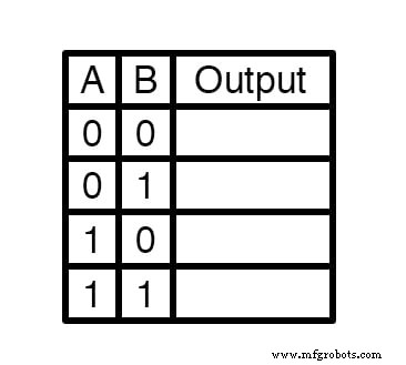
The columns labeled “A” and “B” represent the two input switches; a closed switch indicates a logic “1,” and an open switch (pulled down) indicates a logic “0.” The LED status shows the gate’s output. After completing all four combinations, compare your table to the standard NAND truth table.
While this setup is tailored for the 4011 NAND gate, the same two‑switch, two‑pulldown, LED scheme works for any quad logic IC, provided you consult the correct pin‑out diagram. Remember that pin assignments differ among IC families.
Additional Improvement
To enhance clarity, add LEDs to display the actual input levels. This way, you can verify that a switch is properly closed or opened without inferring from its position:
RELATED WORKSHEET:
- Basic Logic Gates Worksheet
Industrial Technology
- Building an Enabled NAND‑Gate SR Latch: Parts, Design, and Operation
- Fundamental Algebraic Identities: Additive, Multiplicative, and Zero Properties
- Understanding Multiple-Input Logic Gates: Functions, Truth Tables, and Practical Applications
- Understanding TTL NOR and OR Gates: Circuit Analysis and Conversion
- Special-Output Logic Gates: Complementary, Tristate, and Bilateral Switches
- Gate Universality: Replicating Any Logic Function with NAND or NOR Gates
- Demystifying the XOR Gate: The Exclusive‑OR Function in Digital Logic
- Thyristors: Types, Operation, and the Power of Silicon Controlled Rectifiers (SCRs)
- Digital Logic Gates Explained: Types, Functions & Applications
- The Definitive Guide to Logic Gate Truth Tables