


Insulated‑Gate Field‑Effect Transistors (MOSFETs) – Design, Operation, and Power Variants
The Insulated‑Gate Field‑Effect Transistor (IGFET), commonly called a Metal‑Oxide‑Semiconductor Field‑Effect Transistor (MOSFET), is a leading variant of the field‑effect transistor family. In contemporary electronics, MOSFETs dominate digital integrated circuits, with each chip often containing up to hundreds of millions of individual devices. Their dimensions routinely fall below one micron, shrinking roughly every 18 months as Moore’s Law persists. While discrete bipolar junction transistors (BJTs) remain more common in standalone packages, large‑area MOSFETs can switch close to 100 A at low voltages, and specialized devices can handle up to 1 kV at lower currents. These transistors occupy a substantial fraction of a square centimeter of silicon, underscoring their significance in power‑constrained systems.
MOSFET Operation
A MOSFET shares the source, gate, and drain terminals of a conventional FET, but the gate is insulated from the silicon by a thin oxide layer. The gate structure resembles a Metal‑Oxide‑Semiconductor (MOS) capacitor—when charged, the gate induces an inversion layer that conducts between source and drain. For an n‑channel device, a positive gate bias attracts electrons into the p‑type substrate, forming an inverted n‑type channel that bridges the heavily doped source and drain. The result is a unipolar device where a single carrier type—electrons in this case—provides conduction.
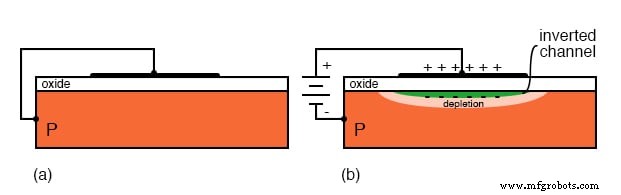
N‑channel MOS capacitor: (a) no charge, (b) charged.
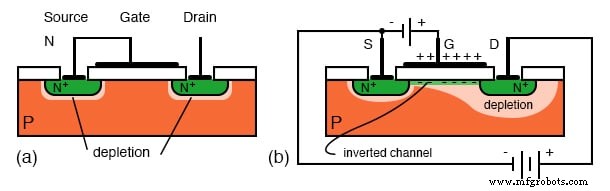
N‑channel MOSFET (enhancement type): (a) 0 V gate bias, (b) positive gate bias. A positive gate bias charges the capacitor, inducing an inversion region that connects the source and drain, allowing a substantial current to flow when a drain‑source voltage is applied. In a practical circuit, the load would be connected in series with the drain supply.
E‑MOSFET (Enhancement Mode)
The configuration described above is an Enhancement‑Mode MOSFET, the most ubiquitous type. The device is normally off; a gate voltage above threshold turns it on by enhancing the inversion channel. Unlike BJTs, the MOSFET’s gate draws no steady current, only a brief surge to charge its capacitance.
Discrete MOSFET Cross‑Section
The cross‑section of a typical n‑channel discrete MOSFET is shown below. Heavy n‑type doping (N+) at the source and drain reduces series resistance, while lighter doping (N−) in the channel region minimizes leakage. The p‑type gate region can be inverted by a positive bias, creating a low‑resistance path from source to drain. Many high‑power devices employ a serpentine layout to increase the effective channel area and current capacity.
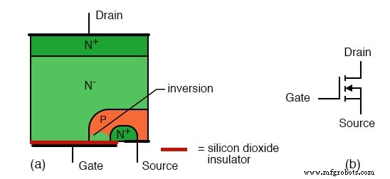
N‑channel MOSFET (enhancement type): (a) cross‑section, (b) schematic symbol.
V‑MOS (V‑Shaped MOSFET)
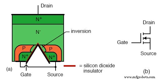
V‑MOS devices feature a V‑shaped gate that expands the source‑drain channel area, reducing on‑state resistance and enabling higher power handling. A U‑shaped variant (UMOS) offers improved manufacturability while preserving performance.
Key Takeaways
- MOSFETs conduct with a single carrier type, making them unipolar like FETs but distinct from BJTs.
- Gate voltage controls source‑to‑drain current; the gate draws virtually no DC current.
- Initial gate charging requires a brief surge, but leakage is negligible.
Related Worksheets
- Conventional Transistor Overview and Special Transistors Worksheet
Industrial Technology
- Designing and Verifying a Basic NAND Gate Circuit with the 4011 IC
- Understanding Junction Field-Effect Transistors (JFETs): Gate Current Direction & N‑Channel vs P‑Channel
- Transistors: IGFET (MOSFET) – Depletion & Enhancement Modes Explained
- CMOS Gate Circuits: Design, Operation, and Comparison to TTL
- Gate Universality: Replicating Any Logic Function with NAND or NOR Gates
- Junction Field‑Effect Transistors (JFET): Design, Operation, and Advanced Variants
- Thyristors: Types, Operation, and the Power of Silicon Controlled Rectifiers (SCRs)
- Understanding Junction Field‑Effect Transistors (JFET): Fundamentals and Applications
- Understanding Insulated‑Gate Field‑Effect Transistors (IGFETs)
- Field-Effect Transistor Biosensors Deliver High Sensitivity and Real-Time Detection Across Healthcare, Food Safety, and Environmental Monitoring