


Accurate Multimeter Testing of JFET Continuity and Pin‑Off Behavior
Testing a JFET with a multimeter can seem simple at first glance, because the device contains only one PN junction—between gate and channel. However, measuring the drain‑to‑source path is a bit more involved, especially when the transistor’s internal capacitance can hold a residual charge that keeps the device pinched‑off even when no external voltage is applied.
Testing Continuity of an N‑channel JFET
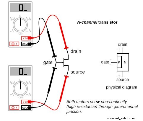
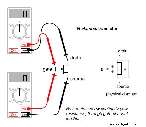
When you test the drain‑source channel, a stored charge on the gate‑channel PN junction may keep the transistor in a pinched‑off state. This means the meter can read a high resistance even though the device is functioning properly. If you already know which pin is the gate, you can short the gate to the source with a jumper wire before testing; this quickly discharges the capacitance and gives you a reliable continuity reading. If the pinout is unknown, the unpredictable charge can make it difficult to identify the correct terminals.
Strategy for Reliable JFET Testing
A proven method is to place the transistor in anti‑static foam just before testing. The foam’s conductivity creates a low‑resistance bridge between all pins, ensuring any residual voltage on the gate‑channel junction is neutralized. Once the device is “opened,” a multimeter will accurately measure the source‑to‑drain resistance.
Because the JFET channel is a single, continuous piece of semiconductor, the source and drain terminals are effectively interchangeable. A resistance check from source to drain (and vice‑versa) should yield the same value—typically a few hundred ohms when the gate‑source voltage is zero. Applying a reverse‑bias voltage across the gate and source will increase the resistance, revealing the pinch‑off characteristic that defines JFET operation.
Following this approach not only guarantees a trustworthy measurement but also protects you from the misleading effects of stored charge. This technique is widely used by electronics technicians and designers who work with low‑noise amplifier stages, where precise JFET characterization is essential.
RELATED WORKSHEETS:
- Junction field‑effect transistors (JFET) Worksheet
Industrial Technology
- Testing Diode Polarity and Forward Voltage with a Multimeter
- How to Identify and Test a Bipolar Junction Transistor (BJT) with a Multimeter
- Using a Junction Field‑Effect Transistor (JFET) as a Low‑Power On/Off Switch
- Expert Guide to JFET Biasing Techniques: Achieve Stable, High‑Performance Circuits
- JFET Transistor Ratings & Package Overview – Choosing the Right Device
- Decoding JFET Quirks: Common Pitfalls & How to Master Them
- Insulated‑Gate Bipolar Transistors (IGBTs): Merging FET Precision with BJT Power
- Understanding Meter Design: From Classic Galvanometers to Modern Digital Displays
- Multimeters: From Analog to Digital – A Comprehensive Guide
- Understanding the TIP120 Transistor: Basics, Features, and Applications