


BJT Biasing Techniques: Mastering Class A, B, AB, C, and D Amplifiers
During the common‑emitter section of this chapter, a SPICE simulation revealed a half‑wave‑rectified output: the transistor failed to remain in its active region during half of the input cycle. To preserve the full waveform, a small bias voltage was introduced, keeping the transistor in the active mode throughout the cycle. This bias voltage is essential for many amplifier classes.
In some scenarios, a half‑wave output is intentional. Certain applications require a specific class of operation—denoted by letters A, B, C, or AB—where the amplifier reproduces only part of the input waveform. Below is a concise overview of each class.
Amplifier Class Overview
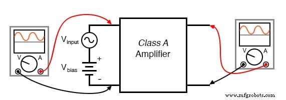
Class A
In Class A, the transistor conducts for the entire input cycle, never reaching cutoff or saturation. A DC bias places the transistor exactly halfway between cutoff and saturation, centering the AC signal between the amplifier’s high and low limits. This yields a faithful reproduction of the input waveform.
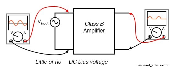
Class B
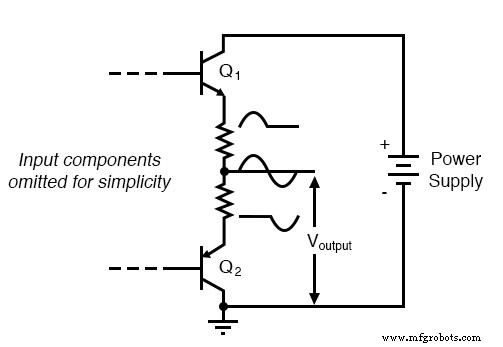
Class B amplifiers were the first to use a common‑emitter configuration without a DC bias. The transistor conducts for only half the cycle, producing a half‑wave output. While a single Class B stage is rarely useful, a push‑pull pair—two complementary transistors—handles positive and negative halves separately. Combined, they recreate the full waveform while offering higher output power and reduced heat dissipation compared to Class A.
Class AB
Class AB sits between Classes A and B. The transistor conducts for more than 50 % but less than 100 % of the cycle, balancing linearity and efficiency. By biasing the base slightly negative relative to Class A, the transistor spends a reduced amount of time in cutoff, yet still avoids the severe distortion of pure Class B.
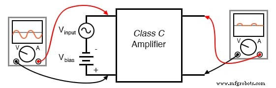
Class C
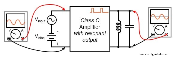
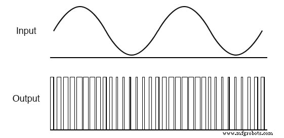
Class C operation conducts for less than half a cycle (<180°). Although the output is heavily clipped, pairing the amplifier with a resonant tank circuit (parallel LC) allows the amplifier’s “kicks” to sustain a high‑frequency oscillation. This configuration is ideal for fixed‑frequency RF transmitters, such as FM radio, where high power efficiency is paramount.
Class D
Class D amplifiers differ fundamentally: the output transistor is driven only in cutoff or saturation, producing a high‑frequency square wave whose duty cycle matches the input amplitude. After low‑pass filtering, the output closely approximates the original waveform. This topology minimizes heat dissipation and achieves very high efficiency, making it common in high‑power audio and industrial inverter applications.
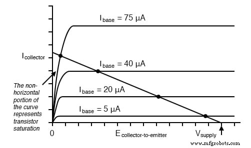
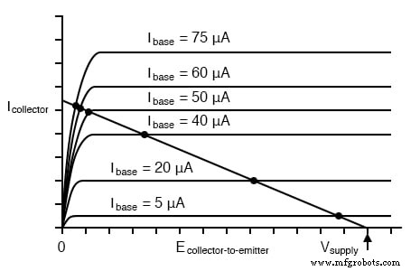
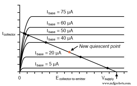
Quiescent Current and Load Lines
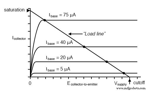
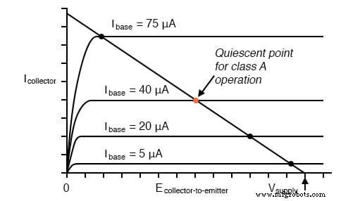
Quiescent current is the steady current flowing when the input is zero. In Class A, it equals half the saturation current; Classes B and C have zero quiescent current; Class AB sits just above cutoff. A load line—graphing collector‑emitter voltage against collector current—illustrates the transistor’s operating point for a given load resistance. For Class A, the quiescent point lies at the midpoint of the load line, ensuring linear operation and avoiding saturation.
Practical Biasing with Voltage Dividers
Using a separate battery to provide bias is impractical because battery voltage drifts over time. Instead, a voltage divider across the main supply can generate the required bias. For example, with a 15 V supply, selecting R₂ = 8.466 kΩ and R₃ = 1.533 kΩ yields 2.3 V across R₃. However, placing the AC input directly across R₃ would short the bias voltage. A coupling capacitor between the signal source and the divider blocks DC while passing the AC, enabling proper biasing.
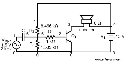
Superposition analysis shows the AC component passes through the capacitor to R₃, while the DC divider remains isolated during biasing. The resulting bias is approximately 2.3 V DC plus the 1.5 V AC signal, as desired.
SPICE simulation of the divider‑biased amplifier:
voltage divider biasing
vinput 1 0 sin (0 1.5 2000 0 0)
c1 1 5 100u
r1 5 2 1k
r2 4 5 8466
r3 5 0 1533
q1 3 2 0 mod1
rspkr 3 4 8
v1 4 0 dc 15
.model mod1 npn
.tran 0.02m 0.78m
.plot tran v(1,0) i(v1)
.end
The initial simulation shows distortion due to loading of the voltage divider by the transistor’s base. Adjusting R₂ and R₃ (e.g., R₂ = 6 kΩ, R₃ = 4 kΩ) restores the 2.3 V bias and eliminates distortion.
voltage divider biasing
vinput 1 0 sin (0 1.5 2000 0 0)
c1 1 5 100u
r1 5 2 1k
r2 4 5 6k  <--- R2 decreased to 6 k
r3 5 0 4k  <--- R3 increased to 4 k
q1 3 2 0 mod1
rspkr 3 4 8
v1 4 0 dc 15
.model mod1 npn
.tran 0.02m 0.78m
.plot tran v(1,0) i(v1)
.end
Key Takeaways
- Class A – Full‑cycle conduction; accurate waveform reproduction; high heat dissipation.
- Class B – Half‑cycle conduction; efficient when paired as push‑pull; suitable for high‑power audio.
- Class AB – Hybrid; balances linearity and efficiency.
- Class C – Ultra‑efficient for fixed‑frequency RF; requires resonant tank circuit.
- Class D – High‑frequency PWM; minimal active‑mode dissipation; excellent efficiency for audio and industrial inverters.
- Biasing via voltage dividers with coupling capacitors is preferred over external batteries for stability.
Related Worksheets
- Bipolar Transistor Biasing Circuits Worksheet
- Class A BJT Amplifiers Worksheet
- Class B BJT Amplifiers Worksheet
- Bipolar Junction Transistor (BJT) Theory Worksheet
Industrial Technology
- Bipolar Junction Transistors (BJT): Core Principles and Practical Applications
- BJT Switching: How Transistors Efficiently Control High‑Current Loads
- How to Identify and Test a Bipolar Junction Transistor (BJT) with a Multimeter
- Precision Transistor Biasing: Calculating Resistors for Stable Amplifier Performance
- Essential Transistor Ratings and Package Types for Bipolar Junction Transistors
- Common-Emitter Amplifier Limitations: Distortion, Temperature, and High‑Frequency Challenges
- Expert Guide to JFET Biasing Techniques: Achieve Stable, High‑Performance Circuits
- Expert Guide to Biasing Techniques for IGFETs
- Insulated‑Gate Bipolar Transistors (IGBTs): Merging FET Precision with BJT Power
- Master BJT Biasing: Techniques, Tips, and Troubleshooting for Reliable Amplification