


Precision Transistor Biasing: Calculating Resistors for Stable Amplifier Performance
Transistor switching circuits can function without bias, but almost all analog designs rely on a carefully set bias point. This guide walks through the most common biasing topologies—base‑bias, collector‑feedback, emitter‑bias, and voltage‑divider bias—and shows how to choose resistor values to achieve a target emitter current while minimizing sensitivity to temperature, β variation, and supply tolerance.
Base‑Bias Resistor
In the simplest configuration a resistor, R_B, connects the base to a bias supply, V_{BB}. Often we reuse the main supply, V_{CC}, as the bias source. The loop equation is:
\[ V_{BB} = I_B R_B + V_{BE} \]
Assuming a high current gain (\beta\) we set I_C ≈ I_E and use V_{BE} ≈ 0.7 V for silicon transistors.
Example: with \beta = 100 and a desired emitter current of 1 mA, the calculation yields R_B ≈ 930 kΩ. The nearest standard value is 910 kΩ.
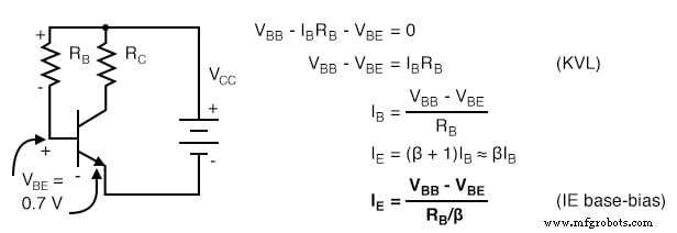
Using the 910 kΩ resistor gives an emitter current close to the target. However, if \beta increases to 300 the emitter current triples, which can be problematic in power amplifiers but is acceptable for low‑level audio signals.
Base‑bias lacks temperature stability: higher emitter current raises device temperature, which further increases current—a runaway effect.
Collector‑Feedback Bias
Connecting the top of R_B to the collector introduces negative feedback. An increase in emitter current raises V_C, lowering base current and correcting the rise.
The loop equation becomes:
\[ V_{CC} = I_C R_C + I_B R_B + V_{BE} \]
Solving for I_E gives the collector‑feedback bias equation.
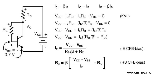
Example: with 1 mA target, 4.7 kΩ collector load, and \beta = 100, the required feedback resistor is about 460 kΩ (use 470 kΩ). Recalculating shows improved stability: emitter current shifts from 0.989 mA to 1.48 mA when \beta rises to 300—half the variation seen with base‑bias.
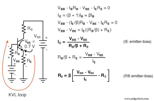
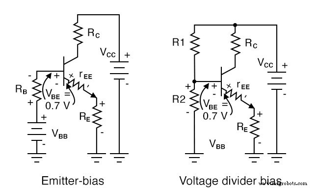
Emitter‑Bias (Degeneration)
Adding an emitter resistor R_E introduces negative feedback that counters changes in current due to temperature, supply ripple, or device variations. The voltage drop across R_E opposes changes in base current, thereby stabilizing the emitter current.
Key design steps:
- Choose
R_Cto setV_C ≈ V_{CC}/2. - Select
R_Earound 10–50 % ofR_Cfor effective degeneration. - Calculate the Thevenin equivalent of the base network to find
R_B.
R_B ≈ 910 kΩ for a 1 mA current with R_E = 470 Ω. Reducing the base bias supply to 2 V and using a 910 Ω emitter resistor brings the current for \beta = 300 down to 1.25 mA, an improvement over base‑bias.
Including the transistor’s internal emitter resistance (r_{EE} ≈ 26 mV/I_E) slightly lowers the required base resistor to about 80 kΩ.
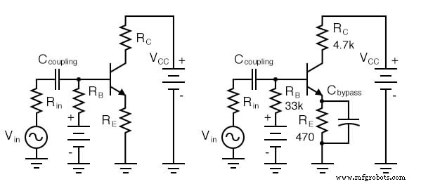
Bypass Capacitor for R_E
While R_E stabilizes DC operation, it also reduces AC gain by creating emitter degeneration. A bypass capacitor C_B short‑circuits R_E for signal frequencies, restoring AC gain.
Rule of thumb: X_C = 1/(2πfC_B) ≤ 0.1 R_E for the lowest frequency of interest. For an audio amplifier covering 20 Hz–20 kHz, a 2 µF capacitor satisfies this criterion.
Voltage‑Divider Bias
Replacing the dedicated bias supply with a voltage divider made from the main supply offers robust biasing. The divider’s Thevenin equivalent supplies a stable V_{th} and resistance R_{th} to the base.
Procedure:
- Start with a proven emitter‑bias design.
- Apply Thevenin’s theorem to find
V_{th}(open‑circuit voltage) andR_{th}(parallel of the two divider resistors). - Set
R_{th} = R_Bfrom the emitter‑bias calculation. - Compute
R_1andR_2using the voltage‑divider ratio.
V_{CC}=10 V yields R_1 = 220 kΩ and R_2 = 39 kΩ, which maintain the target emitter current.
Key Takeaways
- Select the bias topology that matches the required current and stability.
- Base‑bias is simple but highly sensitive to
βand temperature. - Collector‑feedback offers better
βstability but still varies with supply. - Emitter‑bias provides the best DC stability; add a bypass capacitor for AC gain.
- Voltage‑divider bias gives a compact, reliable bias network driven by the main supply.
- Always verify with the nearest standard resistor values and recalculate currents.
For deeper practice, try the worksheet: Class A BJT Amplifiers Worksheet.
Industrial Technology
- Using a Transistor as an Electrically Controlled Switch
- Sensitive Static‑Electricity Detector Using a JFET Switch
- Bipolar Junction Transistors (BJT): Core Principles and Practical Applications
- BJT Switching: How Transistors Efficiently Control High‑Current Loads
- BJT Biasing Techniques: Mastering Class A, B, AB, C, and D Amplifiers
- Insulated‑Gate Bipolar Transistors (IGBTs): Merging FET Precision with BJT Power
- Understanding the Shockley Diode: A Comprehensive Guide to PNPN Thyristors
- Calculating Voltage and Current in Reactive DC Circuits
- Advanced Analysis of DC Reactive Circuits with Non‑Zero Initial Conditions
- Understanding Six Primary Leakage Mechanisms in MOS Transistors