


Understanding Six Primary Leakage Mechanisms in MOS Transistors
Leakage current can significantly contribute to power dissipation, especially as devices scale to lower threshold voltages. Below we examine the six most common leakage paths in modern MOS transistors.
In short‑channel MOSFETs, the following leakage mechanisms dominate:
- Reverse‑bias p‑n junction leakage
- Subthreshold leakage
- Drain‑induced barrier lowering (DIBL)
- Threshold‑voltage roll‑off
- Temperature dependence
- Gate‑oxide tunneling (direct and Fowler‑Nordheim)
- Hot‑carrier injection into the gate oxide
- Gate‑induced drain lowering (GIDL)
- Punch‑through leakage
Familiarity with basic MOSFET operation will help you understand the nuances of each mechanism.
1. Reverse‑Bias p‑n Junction Leakage
During normal operation, the drain‑source and substrate junctions of a MOSFET are reverse‑biased. Leakage in these junctions arises from minority‑carrier drift/diffusion and avalanche generation. Its magnitude depends on doping concentration and junction area. In heavily doped regions, band‑to‑band tunneling (BTBT) becomes the dominant leakage path, especially under electric fields exceeding 10⁶ V/cm.
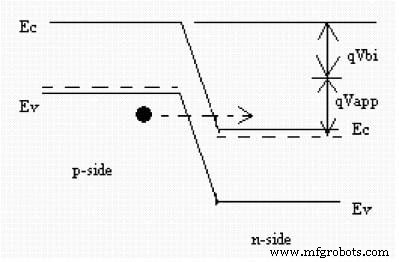
Figure 1. Band‑to‑band tunneling in a reverse‑biased p‑n junction of a MOS transistor. Courtesy: K. Roy et al., “Leakage current mechanisms and leakage reduction techniques in deep‑submicrometer CMOS circuits,” IEEE Proc., vol. 91, no. 2, Feb 2003.
2. Subthreshold Leakage
When the gate voltage is below the threshold voltage (Vth) yet above zero, the transistor operates in the weak‑inversion region. Minority carriers still exist, and for |VDS| > 0.1 V the entire voltage drop occurs across the drain‑substrate junction, resulting in a diffusion‑dominated current.
Drain‑Induced Barrier Lowering (DIBL)
In short‑channel devices, the depletion regions of the drain and source overlap, lowering the potential barrier at the source. This allows carriers to inject into the channel even when VGS < Vth, increasing subthreshold leakage. DIBL is more pronounced at high drain voltages.
Threshold‑Voltage Roll‑Off
Shortening the channel reduces Vth because the depletion regions intrude further into the channel, effectively reducing the gate voltage required for inversion. Lower Vth directly amplifies subthreshold current, which scales roughly as 1/Vth.
Temperature Dependence
Elevated temperatures decrease Vth and increase carrier thermal velocity, leading to higher subthreshold leakage. Designers must account for this effect when specifying temperature margins.
3. Gate‑Oxide Tunneling Leakage
Ultra‑thin gate oxides (≤ 1.5 nm) generate electric fields strong enough for electrons to tunnel from the substrate to the gate and vice versa. Two primary tunneling mechanisms exist:
- Fowler‑Nordheim tunneling – electrons cross a triangular barrier.
- Direct tunneling – electrons cross a trapezoidal barrier.
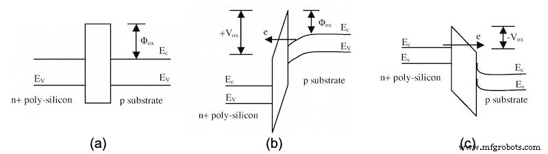
Figure 2. Energy band diagrams of a MOS transistor in flat‑band (a), positive gate bias (b), and negative gate bias (c) conditions.
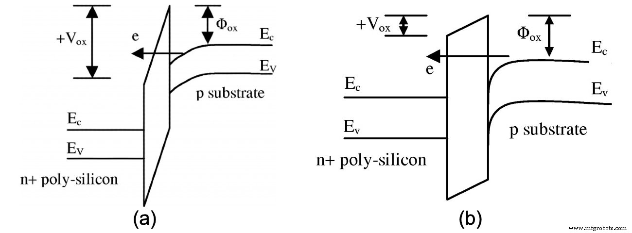
Figure 3. (a) Fowler‑Nordheim tunneling through a triangular barrier; (b) Direct tunneling through a trapezoidal barrier.
4. Hot‑Carrier Injection
Near the source‑channel junction, high electric fields can accelerate carriers to energies exceeding the Si/SiO₂ band offset. These hot carriers cross the interface into the gate oxide, causing a gradual increase in leakage and eventual device degradation.
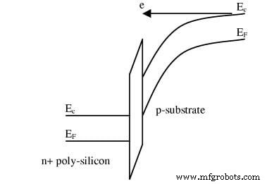
Figure 4. Energy band diagram illustrating hot‑carrier injection from the channel into the gate oxide.
5. Gate‑Induced Drain Lowering (GIDL)
In an NMOS on a p‑type substrate, a negative gate voltage accumulates holes at the gate‑oxide interface, effectively doping the surface more heavily. This creates a thin depletion region along the drain‑substrate interface, enhancing the electric field. The high field triggers avalanche multiplication and BTBT, generating minority carriers that are driven into the substrate, adding to leakage.
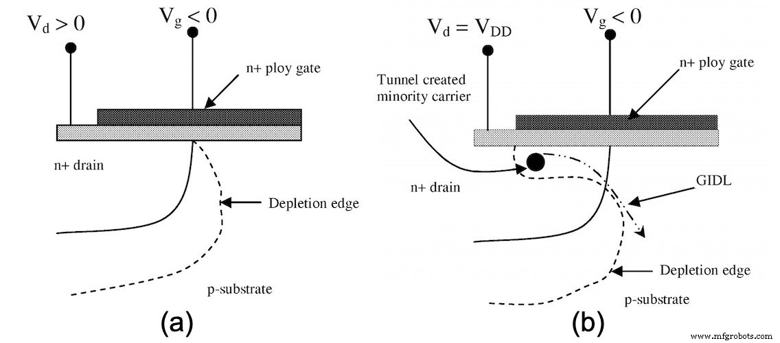
Figure 5. (a) Thin depletion region at the drain‑substrate interface; (b) GIDL current flow via avalanche and BTBT mechanisms.
6. Punch‑Through Leakage
When the depletion regions of the drain and source overlap completely, the potential barrier between them collapses. This punch‑through effect allows carriers from the source to traverse directly into the substrate and potentially reach the drain, causing a significant leakage path.
Understanding these six leakage mechanisms is essential for designing low‑power, high‑performance MOS devices. For further discussion, feel free to leave a comment below.
Embedded
- Hands‑On Guide to Current Dividers: Build, Measure, and Simulate with a 6 V Battery
- Using a Transistor as an Electrically Controlled Switch
- Sensitive Static‑Electricity Detector Using a JFET Switch
- Bipolar Junction Transistors (BJT): Core Principles and Practical Applications
- BJT Switching: How Transistors Efficiently Control High‑Current Loads
- Precision Transistor Biasing: Calculating Resistors for Stable Amplifier Performance
- Insulated‑Gate Bipolar Transistors (IGBTs): Merging FET Precision with BJT Power
- Understanding the Shockley Diode: A Comprehensive Guide to PNPN Thyristors
- Decoding Leakage Currents in Short‑Channel MOS Transistors: Key Insights for Low‑Power Design
- Advanced Method Detects Transistor Defects with Unprecedented Sensitivity