


How to Identify and Test a Bipolar Junction Transistor (BJT) with a Multimeter
Bipolar transistors are fabricated as a three‑layer semiconductor sandwich—either PNP or NPN. When a multimeter is set to the resistance or diode‑check mode, a BJT behaves like two back‑to‑back diodes. This simple test lets you verify the device and identify its pins without a datasheet.
When tested with a typical multimeter that only has a single continuity range, the meter will show low resistance on the base when the negative (black) lead is placed on the base of a PNP transistor. In the transistor symbol, the N‑type material of the base is indicated by the arrow of the base‑emitter junction pointing toward the base. The opposite side of the junction is the P‑type emitter, and the collector is also P‑type.
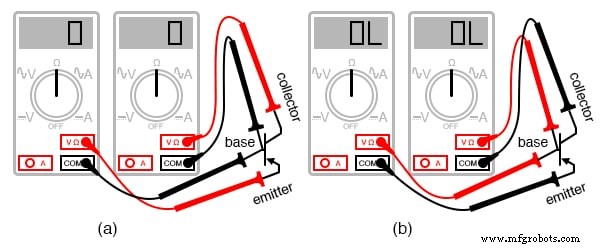
PNP transistor meter check: (a) forward B‑E, B‑C, resistance is low; (b) reverse B‑E, B‑C, resistance is ∞.
Some meters provide a dedicated “diode check” mode. If available, use that instead of the generic resistance setting; the display will then show the actual forward voltage of each PN junction rather than a simple pass/fail reading.
The readings are inverted for an NPN device: a low resistance appears when the red (+) lead is on the base, reflecting the opposite polarity of the base junction.
When the diode‑check mode is used, the emitter‑base junction typically shows a slightly higher forward voltage (≈0.65 V) than the collector‑base junction (≈0.62 V). This difference stems from the heavier doping of the emitter layer, which raises its barrier potential.
Knowing the forward‑voltage difference allows you to determine which pin is which on an unmarked transistor—a critical step because the physical layout of BJT leads is not standardized. All bipolar transistors have three wires, but their positions vary by package type.
Suppose you find an unlabelled transistor and measure continuity with the meter set to diode‑check. The following table records the results:
- Wire 1 (+) & 2 (−): OL
- Wire 1 (−) & 2 (+): OL
- Wire 1 (+) & 3 (−): 0.655 V
- Wire 1 (−) & 3 (+): OL
- Wire 2 (+) & 3 (−): 0.621 V
- Wire 2 (−) & 3 (+): OL
The only pairs that conduct are 1–3 and 2–3, both with the red lead on the first pin and the black lead on the third. These correspond to forward‑biased emitter‑base (0.655 V) and collector‑base (0.621 V) junctions, respectively.
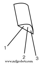
Wire 3 is common to both conducting pairs, so it must be the base. Because the black lead was on wire 3 in the forward tests, the base is N‑type. Therefore the transistor is a PNP with wire 1 as emitter, wire 2 as collector, and wire 3 as base, as illustrated below.
- Emitter & Collector high resistance: 1 (+) & 2 (−): OL
- Collector & Emitter high resistance: 1 (−) & 2 (+): OL
- Emitter & Base forward: 1 (+) & 3 (−): 0.655 V
- Emitter & Base reverse: 1 (−) & 3 (+): OL
- Collector & Base forward: 2 (+) & 3 (−): 0.621 V
- Collector & Base reverse: 2 (−) & 3 (+): OL
Note that the base pin is not always the middle lead, contrary to the simplified “sandwich” diagram. In practice, pin identification must rely on meter checks or the part’s datasheet.
Testing a BJT with a multimeter not only confirms its presence but also reveals whether it is functional. If a device shows conduction in more or fewer than the two expected pairs, it is likely defective or not a BJT at all.
To illustrate how a transistor operates beyond the two‑diode model, consider a simple switching circuit shown below. The small base current that forward‑biases the base‑emitter junction allows a large collector‑emitter current to flow, even though the collector‑base junction is reverse‑biased. This phenomenon is a consequence of the transistor’s internal doping profile and quantum mechanical effects that two isolated diodes cannot replicate.
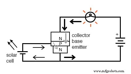
A base current of only a few microamps can open a “gate” for a substantial collector current, as seen when the lamp lights in the circuit.
Early attempts to model a transistor as two series diodes failed because the reverse‑biased collector‑base junction never conducts, regardless of the current flowing through the base. The precise doping ratios and spatial arrangement of the emitter, base, and collector layers are essential for transistor action—an aspect covered in depth in semiconductor physics texts such as “Bipolar Junction Transistors, Chapter 2.”
Key takeaways:
- A multimeter set to resistance or diode‑check mode will show a BJT as two back‑to‑back PN junctions.
- The emitter‑base junction has a slightly higher forward voltage drop than the collector‑base junction due to heavier emitter doping.
- In cutoff, the reverse‑biased collector‑base junction blocks current. A base current “opens the gate,” permitting a limited collector‑to‑emitter current.
For further practice, try the Bipolar Junction Transistor (BJT) Theory Worksheet linked in the related section.
Industrial Technology
- Understanding Ladder Diagrams: Design, Wiring, and Safety in Industrial Control Systems
- Testing Diode Polarity and Forward Voltage with a Multimeter
- Bipolar Junction Transistors (BJT): Core Principles and Practical Applications
- BJT Switching: How Transistors Efficiently Control High‑Current Loads
- BJT Biasing Techniques: Mastering Class A, B, AB, C, and D Amplifiers
- Essential Transistor Ratings and Package Types for Bipolar Junction Transistors
- Common-Emitter Amplifier Limitations: Distortion, Temperature, and High‑Frequency Challenges
- Accurate Multimeter Testing of JFET Continuity and Pin‑Off Behavior
- Insulated‑Gate Bipolar Transistors (IGBTs): Merging FET Precision with BJT Power
- Master BJT Biasing: Techniques, Tips, and Troubleshooting for Reliable Amplification