


Understanding JFET Active‑Mode Operation: From SPICE Simulations to Transconductance
Junction‑field‑effect transistors (JFETs) behave much like bipolar junction transistors (BJTs) in that they can operate in an active regime—between cutoff and saturation—where they regulate current. To illustrate this behavior, we’ll run a SPICE simulation that mirrors the one used to study basic BJT operation.
Spice Simulation of a JFET
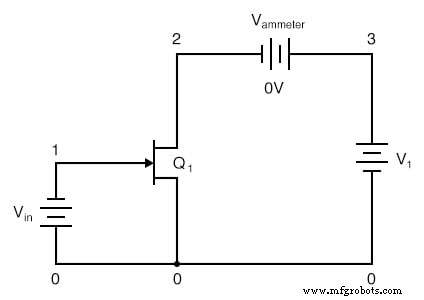
jfet simulation vin 0 1 dc 1 j1 2 1 0 mod1 vammeter 3 2 dc 0 v1 3 0 dc .model mod1 njf .dc v1 0 2 0.05 .plot dc i(vammeter) .end
In the schematic, the transistor labeled “Q1” is written as j1 in the SPICE netlist. While circuit diagrams routinely use the letter “Q” to denote any transistor, SPICE requires a specific prefix to identify the device type: q for BJTs and j for JFETs.
The controlling signal is a steady 1‑V source applied with the negative terminal to the gate and the positive terminal to the source, thereby reverse‑biasing the gate‑source PN junction. Unlike a BJT, which is current‑controlled, a JFET is voltage‑controlled, so a 1‑V gate‑source voltage sets the drain current.
Like a BJT, a JFET keeps the drain current near a fixed value as the supply voltage increases—up to the point where breakdown occurs. To confirm this, we sweep the supply voltage from 0 to 50 V while holding the gate voltage constant.
jfet simulation vin 0 1 dc 1 j1 2 1 0 mod1 vammeter 3 2 dc 0 v1 3 0 dc .model mod1 njf .dc v1 0 50 2 .plot dc i(vammeter) .end
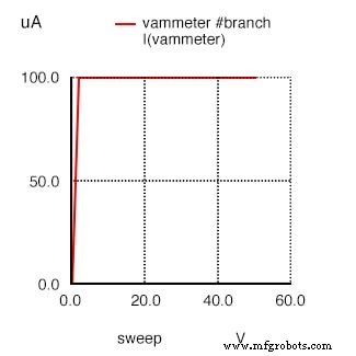
The drain current remains steady at 100 µA regardless of the supply voltage, demonstrating the JFET’s ability to regulate current over a wide voltage range.
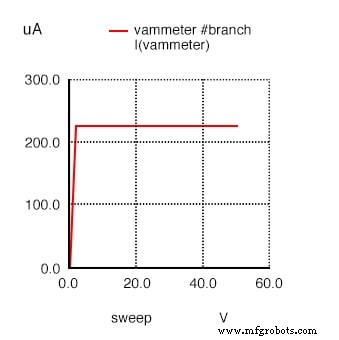
Because the gate voltage controls the channel constriction, adjusting it is the only way to shift the regulated current level—just as varying the base current shifts the collector current in a BJT. Lowering the gate voltage to 0.5 V increases the drain current to 225 µA.
jfet simulation vin 0 1 dc 0.5 j1 2 1 0 mod1 vammeter 3 2 dc 0 v1 3 0 dc .model mod1 njf .dc v1 0 50 2 .plot dc i(vammeter) .end
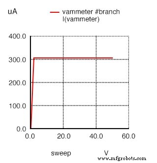
Reducing the gate voltage further to 0.25 V raises the drain current to 306.3 µA, but the relationship is clearly nonlinear: halving the gate voltage does not halve the drain current.
jfet simulation vin 0 1 dc 0.25 j1 2 1 0 mod1 vammeter 3 2 dc 0 v1 3 0 dc .model mod1 njf .dc v1 0 50 2 .plot dc i(vammeter) .end
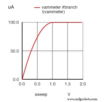
To visualize the nonlinearity more clearly, we hold the supply voltage fixed and vary the gate voltage from 0 to 2 V.
jfet simulation vin 0 1 dc j1 2 1 0 mod1 vammeter 3 2 dc 0 v1 3 0 dc 25 .model mod1 njf .dc vin 0 2 0.1 .plot dc i(vammeter) .end
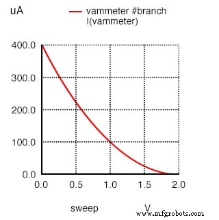
The graph shows that most of the drain‑current reduction (≈ 75 %) occurs within the first 1 V of gate voltage; the remaining 25 % requires an additional full volt. Cutoff occurs at 2 V.
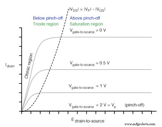
JFET Characteristic Curves
The characteristic curves illustrate the same current‑regulating behavior seen in BJTs, but the spacing between curves reveals the JFET’s nonlinearity.
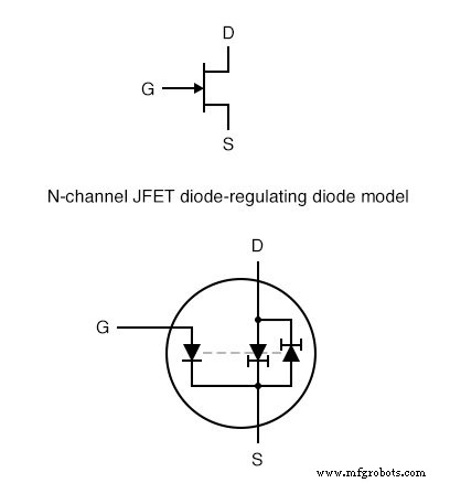
A useful mental model replaces the JFET with a pair of constant‑current diodes whose reference current is set by the reverse‑biased gate‑source voltage. Because the channel is unipolar, the device is bilateral—current can flow in either direction between source and drain.
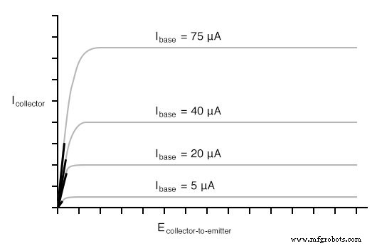
When we compare the JFET’s curves to those of a BJT, the linear (non‑horizontal) portions of the JFET’s curves are noticeably longer.
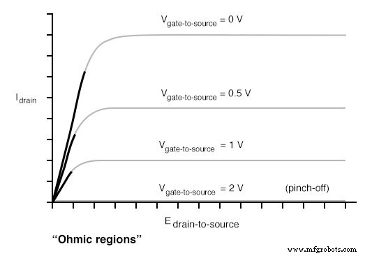
In the triode region, a JFET behaves like a plain resistor; its drain‑to‑source current is directly proportional to the drain‑to‑source voltage. This ohmic behavior can be exploited in circuits that require a voltage‑controlled resistance.
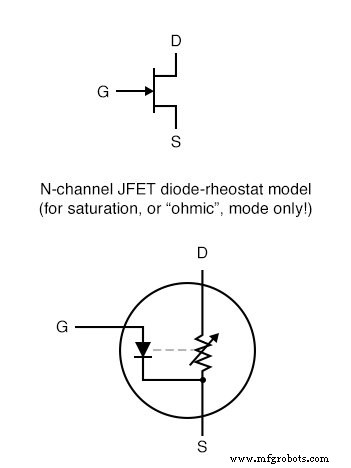
Here the rheostat model applies only over a narrow voltage range where the device is deeply saturated. The resistance is set by the gate‑source voltage: a smaller reverse bias yields a lower resistance (steeper slope).
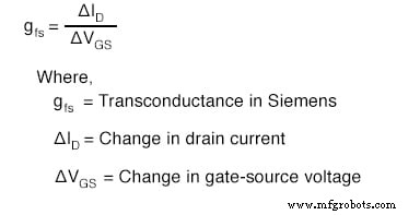
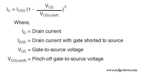
Because JFETs are voltage‑controlled current regulators in the active region, they do not possess a single current‑gain factor like BJTs. Instead, their performance is quantified by transconductance (gm), measured in Siemens, which represents the ratio of drain current change to gate‑source voltage change.
Transconductance is not constant; it varies with gate voltage, as illustrated by the quadratic equation:
Consequently, the drain current versus gate voltage relationship is inherently nonlinear, as shown by the SPICE simulation.
Review
- In active mode, a JFET regulates drain current through the reverse‑biased gate‑source voltage, analogous to a BJT’s base current control.
- The drain current versus gate voltage relationship is nonlinear; transconductance changes across the operating range.
- In the triode region, a JFET acts as a voltage‑controlled resistor, with resistance set by the gate‑source bias.
Related Worksheets
- Junction field‑effect transistors (JFET) Worksheet
Industrial Technology
- Exploring Voltage Addition with Series Battery Connections
- Voltage Divider Lab: Design, Measurement, and Kirchhoff’s Voltage Law Verification
- Thermoelectricity: Understanding Thermocouples and the Seebeck Effect
- Potentiometric Voltmeter: Precise Voltage Measurement with Minimal Loading
- Understanding BJT Active‑Mode Operation: From Cut‑Off to Saturation
- Decoding JFET Quirks: Common Pitfalls & How to Master Them
- Understanding Active-Mode Operation in IGFETs: Design, Performance, and Applications
- Tachogenerators: Precision Speed Measurement for Industrial Motors and Equipment
- Understanding AC Waveforms: Sine Waves, Frequency, and Oscilloscope Basics
- Understanding Mutual Inductance and Transformer Fundamentals