


Create Gerber Files from Any PCB Design Software – A Complete Guide
No one needs a delayed printed circuit board (PCB) order. The ideal circumstance is that you send your design file to PCB manufacturer, then the manufacturer arranges board fabrication based on your file and deliver products to you. The practical situation, however, is not that simple.
It usually takes such a long period of time from the moment you send your designed file out to your boards' final arriving. Your dissatisfaction towards your PCB manufacturer will rise as turn time increases. Actually, there's much you can do to cut this time period during the whole procedure from your perspective. After all, it's effectiveness and efficiency that account for you.
Gerber files do play a crucial role as a connector and translator between PCB design engineers and PCB manufacturers, enabling design engineers' considerations and concepts to be understood by manufacturers so that correct and reliable products can be effectively and efficiently manufactured.
Definition and Necessity of Gerber Files
Initially developed by a company with the name of Gerber, Gerber format currently refers to a widely accepted standard PCB industry software sticks to, capable of describing circumstances of board images such as conductor layers, soldermask layers, legend layers.
Printed circuit boards are designed in a specialized EDA (Electronic Design Automation) or a CAD (Computer-Aided Design) system that further generate board manufacturing data based on which circuit board fabrications are commenced. PCB manufacturers won't fully understand all details of a PCB design file unless Gerber format file is contained in it as reference and guidelines. Gerber format file is applied to describe design requirement of each image of a circuit board and it can be applied for both bare board fabrication and PCB assembly.
When it comes to bare board fabrication, Gerber format is called for by both standard photoplotters and other manufacturing equipment desiring image data like legend printers, direct imagers or AOI (Automated/Automatic Optical Inspection) equipment etc. put it simply, Gerber format files have to be depended from beginning to the end of PCB fabrication process.
When it comes to PCB assembly, a stencil layer is included in Gerber format and component locations are regulated as well, which will be regarded as significant reference data for SMT (Surface Mount Technology) assembly, thru-hole assembly and mix of them.
Versions of Gerber Files
Nowadays, three versions of Gerber formats are available:
• Gerber X2 - the newest Gerber format with stackup data and attributes contained.
• RS-274-X - an expanded version of Gerber format and it has been widely applied.
• RS-274-D - the oldest version of Gerber format which is being gradually replaced by RS-274-X.
Gerber Files Generation
PCB design engineers should never be too lazy to generate their own Gerber files for the following two reasons.
You are hardly able to make sure the PCB design software you're using is the same as that is being used by your PCB manufacturer. If your PCB manufacturer uses different PCB design software, you have to generate Gerber files by yourself, further conversation and confirmation will definitely cause more time and delay the production process accordingly.
Even if PCB manufacturer uses the same PCB design software as you do, you are still advised to generate Gerber files on your own since difference in terms of applied software may also lead to possible errors.
Therefore, in order to ensure delivery time and reliability of end products, PCB design engineers should learn to generate Gerber files on their own. Gerber files generally contain design data of conductor layer, soldermask layer and silkscreen layer. Furthermore, when it comes to two layers with the same design data, Gerber files should be still generated respectively to avoid possible misunderstanding.
Different PCB design software feature different operation steps of Gerber files generation. In the following part of this article, Gerber files generation methods will be displayed concerning PCB design software.
Altium Designer
With your .pcb file opened with Altium Designer software, click File>>Fabrication Outputs>>Gerber Files sequently. Then, Gerber Setup dialogue window will come out, in which five items are available for engineers to set corresponding parameters in their Gerber files: General, Layers, Drilling Drawing, Apertures and Advanced.
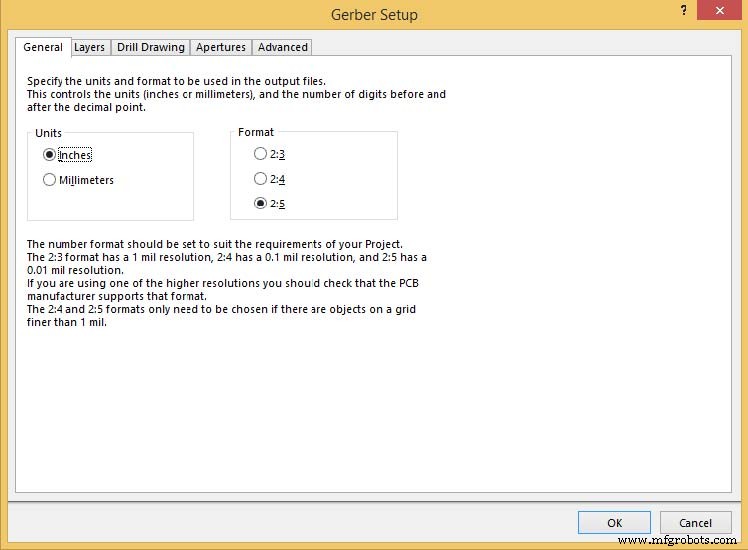
• General button
Under General button, two parameters should be determined: Units and Format. For Units, either Inches or Millimeters can be selected. For Format, three alternatives are supplied. The highest resolution is 2:5 whereas the lowest resolution is 2:3.
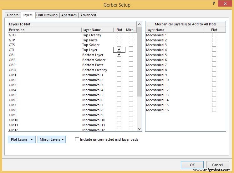
• Layers
In this tab, layers to plot and to mirror should be determined. Cross can be marked at the end of layers that need to be plotted or mirrored. Mechanical layers to add to all plots can be neglected.
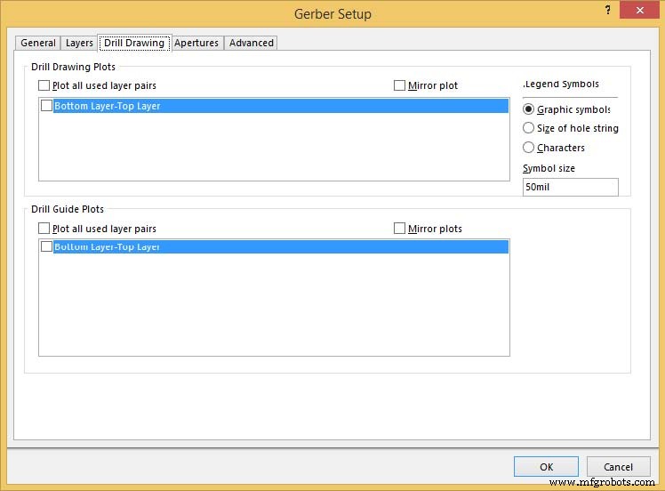
• Drill Drawing
Little should be done in this tab and Legend symbols don't matter much.
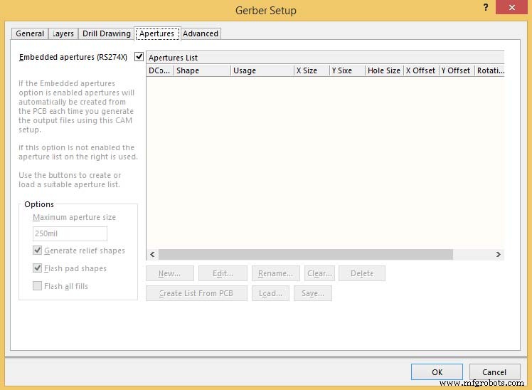
• Apertures
Based on the discussion talked about previously in this article, Embedded apertures (RS274X) should be ticked with other items becoming grey and no further actions are required.
• Advanced
Parameters in Film Size can be set as default by Altium Designer and error may be caused if these parameters are set to be too small. Parameters in Aperture Matching Tolerances, both Plus and Minus should be set to be 0.005mil.
In Batch Mode item, Separate file per layer should be selected.
Leading/Trailing Zeroes, Position on Film and Plotter Type should be selected based on PCB design engineers' preference and demands of specific projects. Leading/Trailing Zeroes and Position on Film determined in Gerber Files should be compatible with that in NC Drill Files.
Among selections in Other item, it is suggested that Optimize change location commands and Generate DRC Rules export file (.RUL) be ticked while the other two selections not.
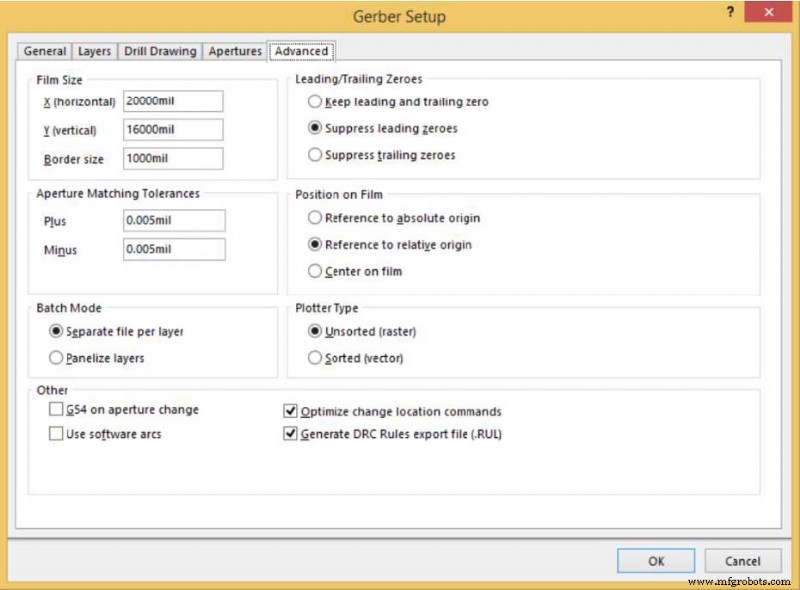
After all the parameters have been determined, press OK button to complete Gerber file generation.
Cadence (Allegro)
Open your PCB layout in Allegro and click Manufacture>>Artwork sequently. Then Artwork Control Form will be seen.
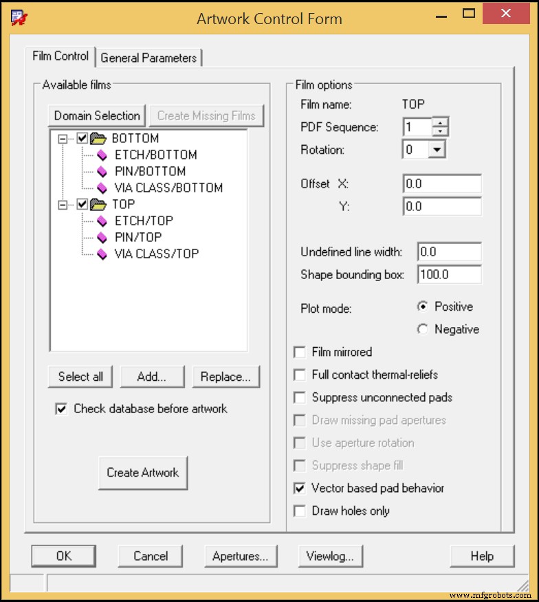
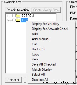
Then it's time to add a board outline by right-clicking on the TOP folder and picking Add Manual.
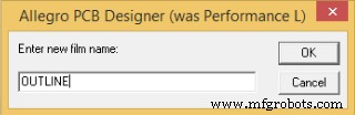
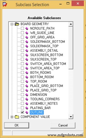
Determine a film name, OUTLINE for example and click OK.
In the Subclass Selection window, expand BOARD GEOMETRY and tick in front of OUTLINE. Then, click OK button.
Back to Artwork Control Form window, tick in front of OUTLINE if it has stayed in the area of Available films.
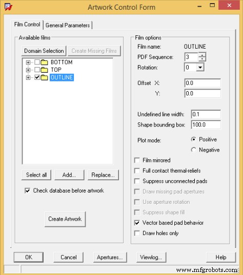
With those steps finished, press Select all button with all the layers output. Then, Gerber files will be generated when Create Artwork button is clicked.
EAGLE
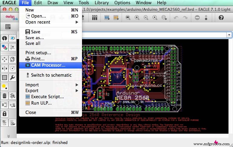
Open your PCB layout with EAGLE software and click File>>CAM Processor. Then you'll encounter a popup dialog.
In this dialog window, click File>>Open>>Job and open a design file in a new window that is shown below.
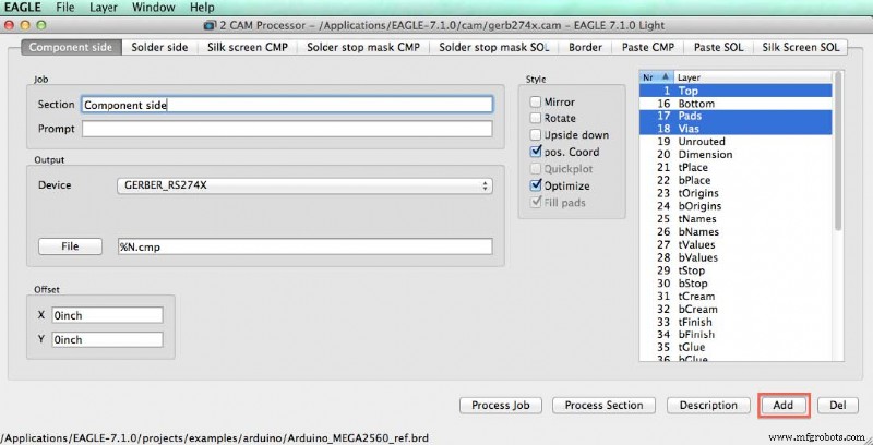
In this window, you should define Gerber files in terms of Component side, Solder side, Silk screen CMP, Solder stop mask CMP, Solder stop mask SOL, Border, Paste CMP, Paste SOL and Silk Screen SOL. As soon as all parameters under all buttons in this window have been determined, you can generate Gerber files by clicking Process Job button.
In my opinion, it's not a difficult job to create a Gerber file in PCB design software as long as you're fully aware of the significance of it for engineers from PCB manufacturers. Remember: create a Gerber file for EACH layer of your PCB together with PCB edge. A clear and integrated Gerber file will definitely drive your order to be effective and efficient.
Industrial Technology
- Choosing the Right PCB Layout Software: Expert Comparison & Recommendations
- How Technology Choices Influence PCB Costs: A Comprehensive Guide
- Master PCB Design: Step‑by‑Step Guide with Pictorial Illustrations
- Master PCB Schematic Design with EasyEDA: A Step‑by‑Step Guide
- Automated Trace Routing in PCB Design: How It Works
- Create NC Drill Files for Your PCB Design Software: A Step‑by‑Step Guide
- From Schematic to PCB: A Comprehensive Altium Designer Workflow
- Preventing Grounding Defects in Control Power Supplies: PCB Design Solutions for Insulation Loss
- Mastering PCB Interference Mitigation: A Professional Guide to Ensuring EMC Compliance
- Understanding PCB Gerber Files: Key Role in Electronics Manufacturing