


PCB Stencil Mastery: The Complete Guide to Precision Solder Paste Printing
The printing phase is the most critical step in PCB assembly. Even a minor mistake can compromise the entire board, so meticulous control over solder joint placement is essential. A PCB stencil eliminates this risk by allowing you to apply solder paste in a single, precise pass, saving time and ensuring consistent quality.
What Is a PCB Stencil?
A stencil is a thin sheet, usually metal or polyimide, perforated with a pattern that matches the layout of the PCB pads. When you press the stencil onto the board and apply solder paste, the paste is deposited only through the apertures, leaving a clean, uniform coating on each pad. The result is a reliable mechanical bond and solid electrical connection.
Most PCB pad manufacturers also supply custom stencils. You can order a board together with its matching stencil, ensuring perfect alignment right from the start.
Stencils come in two primary forms: framed and frameless. Framed stencils (glue‑in) are ideal for high‑volume production because they provide smooth aperture walls and tight tolerances. Frameless stencils, which use a tensioning system, are more economical and easier to store, making them suitable for short runs and prototypes.
PCB Stencil Design
Designing a stencil requires careful consideration of several factors to guarantee optimal paste release and joint quality.
Stencil Thickness
Thickness directly affects the volume of paste that fills each aperture. A too‑thin stencil may cause paste to stick to the aperture walls, while a too‑thick stencil can under‑fill the pad.
Aspect Ratio (W/T)
The aspect ratio is the aperture width divided by the stencil thickness. Industry guidelines recommend an aspect ratio of at least 1.5 to ensure sufficient paste flow and retention. For example, a 0.12 mm aperture should be paired with a 0.08 mm thick stencil (0.12/0.08 = 1.5).
Area Ratio
This is the ratio of the aperture area to the aperture wall area. The minimum acceptable area ratio is 0.66; exceeding this value helps reduce edge roughness and improve paste uniformity.
QFP and BGA Pitch Considerations
- QFP with pitch ≤ 0.5 mm: use 0.12–0.13 mm thickness.
- QFP with pitch > 0.5 mm: use 0.15–0.20 mm thickness.
- BGA ball pitch ≥ 1.0 mm: use 0.15 mm thickness.
- BGA ball pitch 0.5–1.0 mm: use 0.13 mm thickness.
SMT Assembly Specifics
For chemical‑etching processes, an aspect ratio of 1:1.5 is recommended; for laser‑cut stencils, aim for 1:1.12.
Aperture Design
The shape and size of apertures influence defect rates such as bridging or solder beads. A well‑designed aperture also helps maintain a gasket seal between stencil and board, reducing contamination.
Alignment
Precision alignment is critical. Install fiducial marks on both the PCB and stencil; these reference points enable automatic alignment systems and manual setup with high repeatability.
Stencil Material
Metal (stainless steel) stencils provide the best edge quality and dimensional stability for high‑volume runs. Polyimide stencils are cost‑effective and suitable for short runs; laser‑cut polyimide can still achieve excellent aperture fidelity.
Solder Paste Quality
Flux composition and alloy choice affect joint strength. Use a paste that matches the component’s lead profile and the board’s pad geometry to avoid under‑ or over‑flow.
Stencil Coating
Special coatings can reduce residual solder on aperture walls, minimize post‑print cleaning effort, and improve paste release. Consider coatings designed for high‑speed production when running large batches.
Specialized Stencil Designs
Boards with copper‑filled pads or through‑hole vias require a “window effect” aperture that limits paste volume and prevents copper lift. Multi‑layer stencils with step‑up or step‑down thicknesses accommodate components of varying pitch and size on the same board.
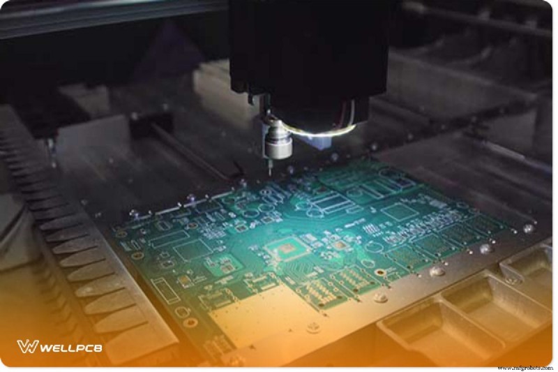
PCB Stencil Manufacturing Methods
Creating precise apertures at scale demands automated processes. The three most common methods are chemical etching, laser cutting, and electroforming.
Laser cutting is the industry standard for high‑resolution stencils, offering smooth walls and zero dust. It is unsuitable for ultra‑tight pitches but works well for pitches down to 0.25 mm.
Laser Cutting Workflow
Key tools: laser cutter, Mylar sheets, CAD software (EagleCAD or ExpressPCB), ViewMate or AutoCAD for Gerber handling, PDF printer, and a DXF viewer.
Step 1: Prepare Mylar Stack
Place two Mylar sheets together. Heat the stack until the top sheet partially melts, allowing the bottom sheet to absorb the melt. Remove the top sheet cleanly, leaving a uniform thickness.
Step 2: Export Design Files
From EagleCAD, export top and bottom cream layers as Gerbers. From ExpressPCB, export a mechanical DXF drawing.
Step 3: Compensate for Melt Shrinkage
In ViewMate, import the Gerbers and use the “Swell” operation to reduce pad dimensions according to the laser’s thermal expansion factor. Save the adjusted file as PDF.
Step 4: Scale DXF in AutoCAD (if needed)
Open the DXF in AutoCAD, select all objects, and apply a scale factor that matches your laser settings. Export the scaled drawing to PDF.
Step 5: Laser Cut
Set the laser parameters (power, speed, frequency) to cut through the Mylar stack. The top sheet will melt slightly; the bottom sheet will absorb the melt, ensuring clean edges. After cutting, separate the sheets and verify aperture quality under magnification.

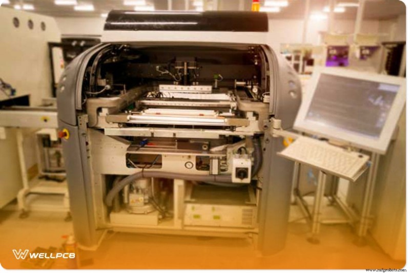
PCB Stencil Printers
High‑precision stencil printers combine repeatability with automated alignment. They come in automatic, semi‑automatic, and manual variants, suitable for everything from prototype runs to full production.
Key features include adjustable squeegee pressure, stroke length, and print speed controls. Integrated camera systems align the stencil to fiducial marks, while vacuum or wet‑dry cycles clean residual paste from the underside.
Conclusion
By mastering stencil design, material selection, and manufacturing techniques, you can eliminate most common printing errors and achieve high‑quality solder joints every time. If you encounter challenges during PCB production, our team of experienced engineers and state‑of‑the‑art equipment are ready to support you.
Industrial Technology
- 9 Proven Steps to Build a Robust Preventive Maintenance Program
- Fluoride‑Based Batteries Offer Up to 8× Longer Lifespan Than Today’s Standards
- University Lawsuit Showcases How Global Supply Chains Are Interlinked
- Riveting vs Welding: Selecting the Best Sheet Metal Join for Strength & Longevity
- Big Data in Manufacturing: 5 Proven Game-Changing Applications
- Unlocking Supply Chain Efficiency: 5 Proven AI Strategies
- Seamless Solar EV Charging with evcc.io on CHARX Control SEC3xxx
- How to Choose Between Filled and Unfilled Wax Processes for Investment Casting Parts
- 2020 Highlights: COVID-19, Careers, and Metalworking – Better MRO’s Top 10 Stories
- 5 Proven Strategies to Make Your Last-Mile Delivery Greener