


Sprint‑Layout: Comprehensive PCB Design Tool – Features, Versions, and Tutorial
Sprint‑Layout is a powerful, user‑friendly PCB design suite that supports single‑, double‑, and multilayer boards. Designed for both hobbyists and professionals, it offers an intuitive interface, robust feature set, and full compatibility with industry‑standard manufacturing files.
Key Features
- Fast, unrestricted layout creation with tracks, pads, zones, text, SMD footprints, and more.
- Export to Gerber (RS‑274X), Excellon, BMP, GIF, JPEG, and HPGL for CNC isolation milling.
- Photoview for realistic, pre‑manufacture inspection.
- Automatic ground planes, signal‑flow testing, and solder‑mask management.
- Extensible component library with pre‑defined through‑hole and SMD parts.
- Advanced printing options for component mounting plans, solder masks, and foil layers.
Version 6.0 Enhancements
- Higher Resolution & Accuracy: Grid settings and zoom factor improved tenfold for intricate designs.
- Pick‑&‑Place Export: Generate .PPL files for automated SMD assembly.
- Anti‑Alias Graphics: Smoother visual representation.
- Multi‑Select & Selector: Edit multiple elements simultaneously with an enhanced selector tool.
- Automatic Capture Mode: Snap-to‑points for precise pad and track placement.
- Gerber Import: Convert existing Gerber files into editable layouts.
- Rubber‑Band Tracking: Maintain track connections while moving components.
- Component Management: Full component list with identifiers and values.
- Thermal Pad Vias: Separate thermal pads per layer.
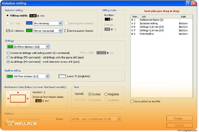
- Isolation Milling: Consolidate milling, drilling, and cut‑out jobs into a single HPGL plot file.
- Grid‑Hotkeys: Quick grid value changes via function keys 1‑9.
- Rectangle & Circular Arrangement Tools: Rapid creation of tracks, zones, and circular patterns.
- Enhanced Crosshair: 45° lines and coordinate display.
System Requirements
Windows XP/Vista/7/8/10 – 1 GB RAM, 400 MB free disk, Intel Pentium 4 or newer.
Export Functions
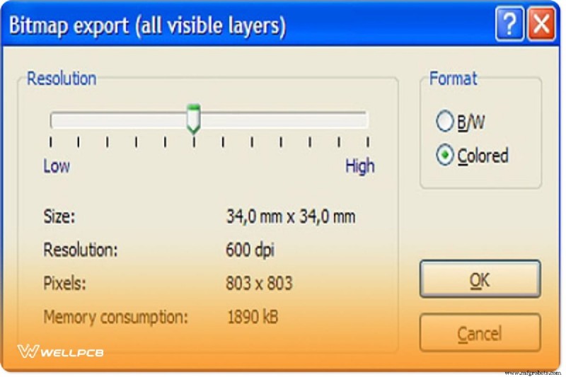
Bitmap‑Export (.bmp)
Creates a bitmap from visible layers, useful for documentation.
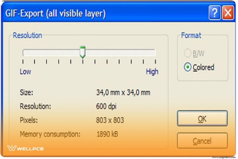
GIF‑Export (.gif)
Compressed image format for web or documentation.
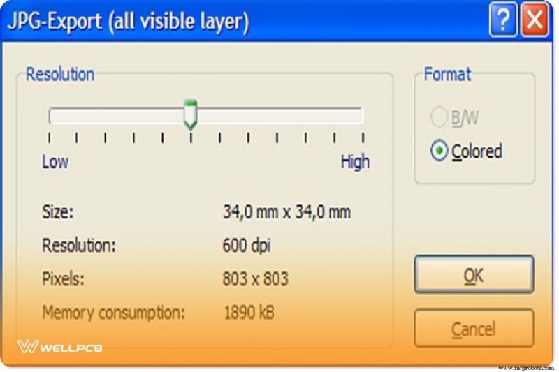
JPEG‑Export (.jpg)
Another compressed option for quick sharing.
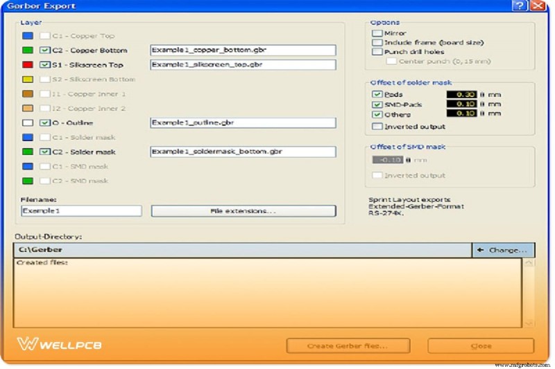
Gerber‑Export (RS‑274X)
Generates standard Gerber files for every layer (copper, solder mask, silkscreen). Essential for professional manufacturing.
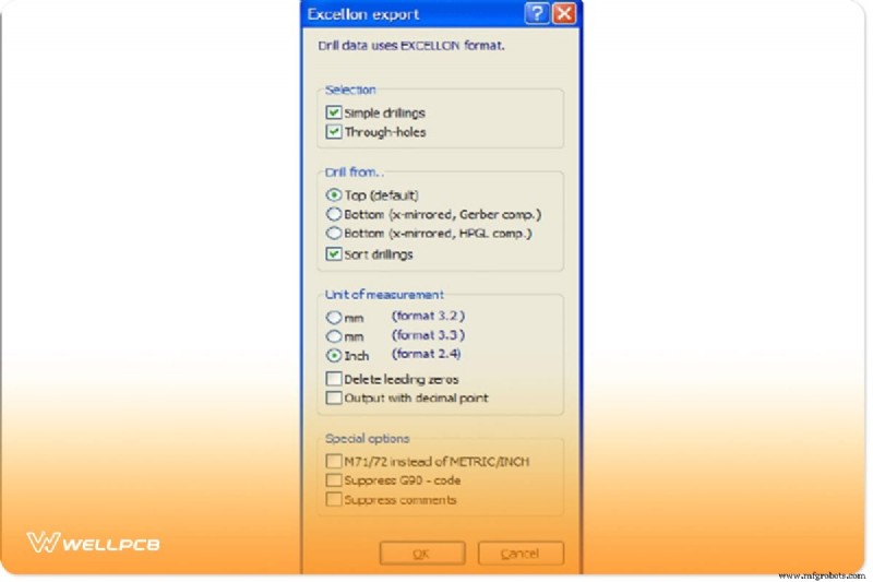
Excellon‑Export
Drill data with diameters and coordinates for CNC drilling.
Isolation Milling (HPGL)
Consolidated plot file for CNC milling of tracks, isolation, drilling, and board outline.
Getting Started – Tutorial Overview
Follow these steps to create and export a complete PCB layout:
- Select the layer you wish to export.
- Click Create Gerber Files.
- Close the dialog once the Gerber files are generated.
- Export drill data via Excellon to include holes.
- Archive all layer files into a ZIP/RAR package.
- Send the package to your chosen PCB manufacturer.
Key tips: avoid the Mirror option; set solder‑mask clearance to 0.5 mm (50 µm) for fine‑pitch components; keep the drill data unit at 2.4 inches.
Professional Perspective
Sprint‑Layout offers a robust CAD experience with a clean UI, hotkey customization, and a dedicated viewer that can calibrate printers for home PCB fabrication. While it lacks an integrated schematic editor (sPlan) and advanced auto‑routing, its simplicity and stability make it a top choice for designers who value speed and reliability.
Read more about sPlan here: Abacom sPlan.
Conclusion
Whether you’re prototyping at home or producing production boards, Sprint‑Layout delivers the tools and export flexibility needed for modern PCB manufacturing. Explore version 6.0’s new features and start your next project today.
Industrial Technology
- Shielded Metal Arc Welding (SMAW): A Comprehensive Guide
- Root Cause Analysis of Blind Via Failures in Empty-Cave PCB Copper Filling
- Meltdown & Spectre Exploits: 8 Essential Insights for Protecting Your Systems
- Expert Guide to PS4 Controller PCB Design, Components, and Purchasing
- Precision Waterjet Cutting: Preserving Metal Panel Integrity
- Mastering Vibration Analysis: A Data‑Driven Strategy to Eliminate Machining Chatter
- Can Automation Threaten the Gig Economy?
- Key Foundations for Successful IIoT Implementation in Your Factory
- How to Choose the Ideal Industrial Pressure Regulator for Your Application
- Deep Hole Drilling & Machining: Key Features, Challenges, and Expert Tips