


Mylar Boards – Mastering Solder Stencil Design for Precise Surface‑Mount Assembly
Mylar Boards – Mastering Solder Stencil Design for Precise Surface‑Mount Assembly
- Last modified on May 12, 2025
- by Hommer Zhao
All‑Round PCB Services
Unbelievable Prices
Speedy and Secure Delivery
Rigorous Vetting and Guaranteed Quality
Five‑Star Custom Care
100 % Money‑Back Guarantee
Secure and Confidential | No Obligation | 10,000+ Quotes Delivered
Introduction
Working with surface‑mount components can be challenging, especially when it comes to soldering the smallest parts. Instead of hand‑soldering each component, the industry standard is to apply solder paste to a stencil, place all components simultaneously, and then reflow the board. The stencil is a thin sheet—commonly made from Mylar—with precisely measured holes that align with the board’s solder pads. Creating a high‑quality Mylar stencil is essential for reliable assembly.
One efficient method for producing these stencils is laser cutting. By using CAD software such as EagleCAD and ExpressPCB, you can export the top and bottom layers of your board design. The laser then carves the Mylar sheets to match the pad outlines.
During the cutting process, the pad outlines are slightly reduced in size to compensate for the thermal expansion that occurs when the laser melts the Mylar. This adjustment prevents the final stencil from being too large, which could cause solder bridging.
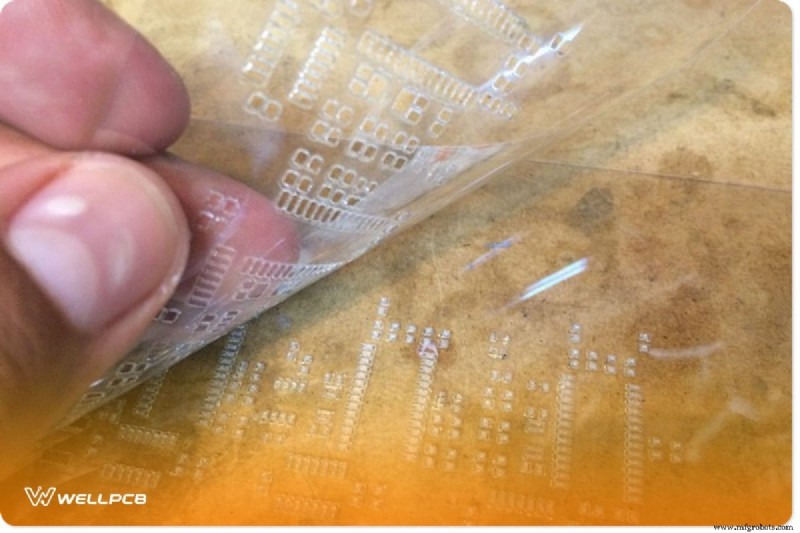
The typical workflow involves cutting two 7‑mil Mylar sheets. The laser is set to fully cut through the top sheet while only partially penetrating the base sheet. This technique softens the edges of the cut‑out squares and allows the two layers to separate cleanly. After cutting, you peel the layers apart, leaving a pristine stencil ready for use and a scrap piece.
RELATED POSTS
Your Trusted PCB Manufacturer & Wiring Harness Provider
Get $100 Off Your First Order!
High‑Quality PCB Manufacturing, Assembly & Wiring Harness Services
Fast Turnaround & Reliable Service
About
Services
Certificates
Delivery Partners
Policies
WellPCB. All rights reserved
Secure and Confidential | No Obligation | 10,000+ Quotes Delivered
Industrial Technology
- What Is Autonomous Maintenance? Boost Efficiency, Reduce Downtime & Empower Teams
- E3.series Database Tutorial: Master Attributes, Connections, & More with Downloads & Courses
- HM-10 Bluetooth Low Energy Module: Complete Technical Guide
- Mastering Ultrasonic Sensor Circuits: The Ultimate Guide
- Optimizing Solar Panel and Battery Wiring: Series-Parallel Configurations Explained
- Unlocking Value: The Key Advantages of Custom Sheet Metal Fabrication
- Build an Automated Warehouse: A Step-by-Step Guide to Modernizing Operations
- Connecting Batteries in Series-Parallel to a Solar Panel: A Step‑by‑Step Guide
- FDA Grants Approval to Ampcare’s Dysphagia Therapy Device
- Shaper Machines Explained: Definition, Components, and Operation