


Optimizing Microstructure and Electrical Performance of CH₃NH₃PbI₃–Cl Perovskite Thin Films via Controlled Precursor Ratios
Abstract
We investigated how varying the molar ratio of lead iodide (PbI₂) to methylammonium iodide (MAI) in the precursor solution—combined with a fixed low level of methylammonium chloride (MACl)—affects the crystallinity, morphology, and electrical properties of CH₃NH₃PbI₃₋ₓClₓ thin films. Increasing the MAI:PbI₂ ratio from 1:1 to 1:2 sharply enhances crystallinity and changes the grain shape from needle‑like to round‑to‑faceted. Beyond 1:2 the crystallinity change is modest, but the grain size continues to shrink. Complex impedance and current‑voltage (I‑V) measurements reveal that charge‑carrier mobility decreases with higher MAI content while conductivity peaks at the 1:2 ratio, illustrating a trade‑off between improved crystallinity and reduced grain size. These findings provide a pathway to tailor perovskite microstructure for high‑efficiency, low‑cost solar cells.
Background
Hybrid organic‑inorganic halide perovskites (APbX₃, A = CH₃NH₃⁺, X = I⁻, Br⁻, Cl⁻) have emerged as leading photovoltaic materials, achieving power‑conversion efficiencies (PCE) exceeding 22 %—surpassing commercial monocrystalline silicon—while remaining inexpensive to produce [1, 2]. Key challenges are ultraviolet degradation and thermal instability, largely driven by defect‑mediated charge recombination at the perovskite/electrode interface [3, 4]. Introducing Cl⁻ or Br⁻ into the lattice can suppress defect formation and improve stability [5, 6]. However, grain boundaries can both trap carriers and facilitate charge separation, and their impact depends on grain size [7, 8]. Consequently, controlling the stoichiometry of the precursor solution offers a direct route to modulate microstructure and electrical performance. This study systematically explores the influence of the PbI₂:MAI ratio on the microstructure and impedance characteristics of CH₃NH₃PbI₃₋ₓClₓ films.
Methods
Synthesis
High‑purity PbI₂, MACl, and pre‑synthesized MAI were dissolved in anhydrous dimethylformamide (DMF) and stirred at 70 °C for 1 h under nitrogen. The resulting solutions (room temperature) were spin‑coated onto cleaned glass substrates (40 rps) and annealed at 70–150 °C for 30 min in a dry box. Three precursor ratios were prepared: 1:1, 1:2, and 1:3 (PbI₂:MAI) with a constant 2 mol % MACl substitution.
Characterization
- Phase analysis: X‑ray powder diffraction (Cu Kα) with DRON‑4‑07 diffractometer.
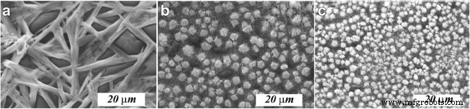
- Microstructure: microinterferometer MII‑4 and SEM (SEC miniSEM SNE 4500MB).
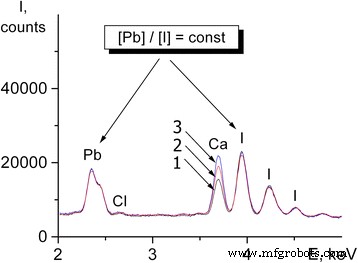
- Composition: EDX (EDAX Element PV6500/00).
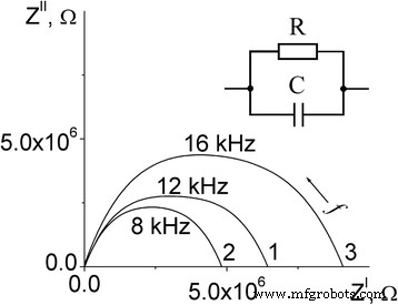
- Electrical: Complex impedance (1 Hz–1 MHz) using Solartron 1260A, and I‑V curves (0–40 V) under dark and 10 mW cm⁻² illumination (0.1 sun). Measurements were performed in dry N₂ (≤ 7 ppm H₂O).
- Data fitting: ZView® for equivalent‑circuit extraction.
Results and Discussions
All films were single‑phase tetragonal (I4/mcm) after annealing at 80 °C, with the 1:2 ratio remaining single‑phase across the temperature range. XRD refinement yielded lattice parameters a = 0.8870 nm, c = 1.2669 nm (V = 0.9968 nm³) [19]. Figure 1 shows the experimental and calculated diffraction patterns for the 1:2 sample.
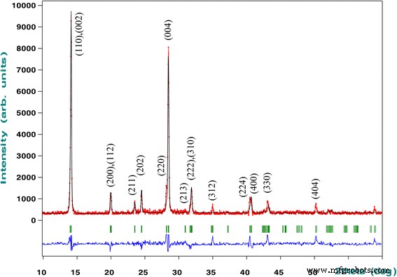
Crystallinity rose sharply as the MAI:PbI₂ ratio increased from 1:1 to 1:2 (Figure 2b) and then plateaued between 1:2 and 1:3. Grain size decreased monotonically with higher MAI content (Figure 4). SEM images reveal a transition from needle‑like grains (1:1) to roundish (1:2) and faceted grains (1:3). Figure 3 presents the EDX spectra confirming the expected elemental ratios.
Impedance spectroscopy in dry N₂ showed a single semicircle in the 8 kHz–80 Hz range, indicative of electronic conduction. Equivalent‑circuit modeling (resistor–capacitor parallel) extracted film resistances and capacitances (Figure 6). The 1:2 ratio exhibited the lowest resistance and highest capacitance, confirming superior electrical performance.
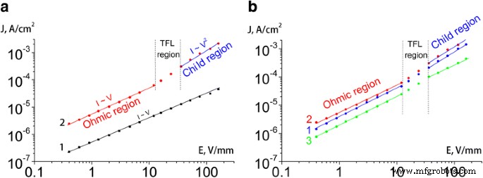
Current density versus voltage plots (Figure 7) revealed linear Ohmic behavior at low bias, a trap‑filled limit (TFL) region at intermediate bias, and a quadratic Child regime at high bias, characteristic of space‑charge‑limited conduction. The 1:2 film achieved the highest conductivity, while mobility decreased with higher MAI content, consistent with reduced grain size.
Conclusions
Varying the PbI₂:MAI precursor ratio profoundly influences the crystallinity, grain morphology, and electrical behavior of CH₃NH₃PbI₃₋ₓClₓ thin films. The 1:2 ratio maximizes conductivity by balancing enhanced crystallinity with an acceptable grain size. Higher ratios reduce mobility due to smaller grains but maintain similar carrier densities under illumination. These insights guide the design of perovskite films with optimized microstructure for next‑generation photovoltaic devices.
Abbreviations
- CPE – Constant phase element
- DC – Direct current
- DMF – Dimethylformamide (C₃H₇NO)
- EDX – Energy‑dispersive X‑ray spectroscopy
- I‑V curves – Current‑voltage curves
- PCE – Power conversion efficiency
- SEM – Scanning electron microscopy
- XRD – X‑ray diffraction
Nanomaterials
- Ultra‑Broadband Terahertz Polarization Control via Anisotropic Dielectric Metasurfaces
- Ultra-Sensitive Large-Scale SERS Substrates: Silver Nanowire Thin Films via Microliter-Scale Solution Coating
- Efficient Ambient‑Air Fabrication of Mesoporous Perovskite Solar Cells Using N‑Butyl‑Amine‑Enhanced PbI₂ Precursors
- Unveiling the Key Factors that Limit Carrier Transport in Ultra‑Thin Amorphous Sn‑Doped In₂O₃ Films with Superior Hall Mobility
- In‑Situ XRD and Electrical Analysis Reveal Phase Transitions and Monolayer Formation in Thin Oligothiophene Films
- Monoclinic V1−x−yTixRuyO₂ Thin Films: Superior Thermal Sensitivity for Microbolometers
- Lowering Energy Barriers: Enhancing Li+ Transport Across Grain Boundaries via Amorphous Domains in LLZO Thin Films
- Skyrmion Phase Realization in MnSi Thin Films Grown on Sapphire via Conventional Sputtering
- Influence of Anisotropy and In‑Plane Grain Boundaries on Cu/Pd Multilayer Films with Cube‑on‑Cube and Twinned Interfaces
- Millport SmartLathez 1740 CNC Lathe – Precision & Power