


Silicon‑Germanium FinFETs: Pioneering Low‑Resistance Channels for 7nm and Beyond
At IBM Research in Albany, NY, our semiconductor team is pushing CMOS technology toward 10 nm, 7 nm, and future nodes. As device dimensions shrink, transistor channel resistance becomes a decisive factor in chip performance. Innovating the channel material to lower that resistance is therefore essential to keep 7 nm and beyond competitive. Our focus is silicon‑germanium (SiGe), the key material that enabled the power‑performance gains highlighted in last year’s 7 nm launch.
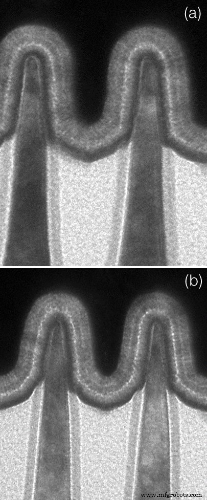
Symmetric Si FinFET (a) and SiGe FinFET (b) profiles at 10 nm, fabricated at SUNY Polytechnic’s NanoTech Complex. SiGe FinFETs exhibit superior electrical properties.
Current 14 nm FinFET chips use silicon‑only channels—silicon’s stability limits beyond this scale. In contrast, SiGe‑based FinFETs have delivered proven performance gains under industry 10 nm standards, offering a practical path to a scalable CMOS technology. One advantage is the ability to integrate both low‑power and high‑performance devices on a single die without compromising either type.
SiGe FinFETs also demonstrate enhanced electrical reliability, translating into more stable chip performance over its lifetime. Consequently, the same process flow serves high‑performance supercomputers and power‑constrained mobile devices alike.
By introducing larger germanium atoms into a silicon lattice, SiGe creates a deliberate lattice mismatch that generates strain in the transistor channel. This strain increases carrier mobility, allowing more current to flow at lower voltages. Thus, SiGe enables a scalable roadmap to smaller dimensions while preserving the power–performance balance.
SiGe for the Nodes Ahead: Solving the Challenges of Producing 10 nm & 7 nm Chips
Maintaining strain throughout the entire integration flow and controlling defect density are the two primary technical hurdles for SiGe FinFETs at 10 nm and below. Strain can be lost during thermal anneals that activate dopants, during source/drain recess steps that form the uniform junction, or during fin patterning in designs requiring ultra‑short fins.
Defect control is equally critical for mass production. The lattice mismatch between a SiGe channel and its silicon substrate makes it difficult to keep defect levels within manufacturable limits across an entire wafer. Through advanced epitaxial growth, innovative fin‑module integration, and refined source/drain engineering, we have achieved strain retention and low defectivity in our 10 nm and 7 nm test nodes.
Building on this feasibility study, we are collaborating with chip designers and foundries to bring SiGe FinFETs to volume production. We anticipate that SiGe will replace silicon FinFETs in next‑generation CMOS nodes, powering everything from supercomputers to mobile devices. The technology also holds promise for “more‑than‑Moore” applications—cloud, cognitive computing, and other low‑power scenarios—where efficient power use is paramount.
Further Reading
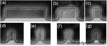
Cross sections of fin and gate stack for fin widths ranging from 87 nm (a) to 3 nm (g) with higher Ge content for SiGe Fin.
At this year’s IEEE VLSI symposium, our teams showcased a suite of device, material, and integration breakthroughs that leverage SiGe under 10 nm ground rules and chart a path to the 7 nm node we fabricated last year. Highlights included defectivity control, gate‑stack and interfacial‑layer innovations tailored for SiGe Fin, and advanced contact techniques—all detailed in our VLSI papers.
- T2.2: “FINFET Technology Featuring High Mobility SiGe Channel for 10 nm and Beyond”
- T4.3: “Selective GeOx-Scavenging from Interfacial Layer on Si1‑xGex Channel for High Mobility Si/Si1‑xGex CMOS Application”
- T9.3: “Replacement High‑K/Metal‑Gate High‑Ge‑Content Strained SiGe FinFETs with High Hole Mobility and Excellent SS and Reliability at Aggressive EOT ~7Å and Scaled Dimensions Down to Sub‑4 nm Fin Widths”
- T7.2: “Ti and NiPt/Ti Liner Silicide Contacts for Advanced Technologies”
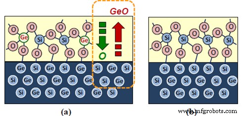
Schematic of the inventive selective GeOx‑scavenging process (a) and the GeOx‑free interfacial layer (b) with SiGe channel.
*‑FinFET refers to a transistor architecture that raises the channel into fin‑like structures.
Dechao Guo is a research staff member, master inventor, and manager of Advanced Device Design & Integration at IBM Research.
Nanomaterials
- Expanding Cloud Horizons: New Zones, Containers, and Multicloud Strategies
- Java vs. C#: 10 Key Differences Explained
- Missouri Technology Corporation Unveils Statewide Initiative to Boost Entrepreneurship and Innovation
- CETMA: Italy’s Premier Composite R&D & Innovation Hub
- Understanding Material Stiffness vs. Strength: Key Differences & Practical Implications
- How IoT & Industrial Automation are Powering Manufacturing Innovation
- AMRC Leads Innovation in Circular Manufacturing & Advanced Recycling Technologies
- ABB Robotics Receives Shanghai Government Award for R&D Innovation
- Advanced 3D Printing Technologies: Part 2 – Exploring Layer‑by‑Layer Manufacturing
- How to Select the Best 3D Printing Technology: FDM, SLA, and SLS Compared